 |
 |
 |

|
|
|

|
Matching the Design Size to an ASIC or FPGAMethods and tools are available to help designers make accurate estimations of gate count and I/O to fit a design into an appropriate device.by Tets Maniwa |
How important is it to target the right ASIC or FPGA for a design? Consider one recent experience at Seva Technologies, Inc., a design and consulting shop.
A customer came to Seva's San Diego operation with a completed design and wanted Seva to implement it in a particular FPGA that the customer had used previously. But when Seva's engineers synthesized the design, it failed to meet timing specifications. The engineers performed several iterations before they were able to meet timing, but by then the design was over twice as large as the original circuit and would no longer fit into the FPGA that the customer had specified. So they were forced to use a different device whose internal architecture was better suited to the original design.
However, if the customer had chosen this type of part originally, Seva could have used a smaller version, since it would have met the timing requirements. But because Seva's engineers had rearchitected the design to add parallelism in an attempt to use the customer's preferred FPGA, the design was now too large for the smaller device, and they had to use the larger one.
The tribulations Seva's engineers underwent, which cost the customer both time and money, illustrate the importance of choosing the right architecture for the application and performance requirements. But deciding on an architecture is only one issue that can have a dramatic impact on the cost of a design and the length of the design cycle.
Accurately estimating the gate count early on allows the designer to choose an appropriate device--in particular, size (number of usable gates or gate equivalents) and packaging. Furthermore, choosing a family of devices that range in package size can also save the designer time and money if the design grows.
Estimating gate counts
An accurate, early estimate of the gate count helps determine the allocation
of the device's resources. In addition, architectural partitions and pin-out
information necessary for the estimate can help the design team assess
the die size and possibly identify physical design constraints, like routing
congestion, early in the design cycle, when design changes have much less
impact on the schedule than they would later.
Unfortunately, estimating gate counts isn't as easy as it sounds. Designers can't use lines of RTL code as a gate estimator, because the number of gates per line of code varies widely. For example, it takes only one line of code to create a wide, complex multiplier, but another line just for the register to hold the result.
There are methods for estimating a design's gate count, ranging from relying on experience to various rules of thumb or the use of synthesis tools. Experienced engineers develop a feel for gate count, and gate array and programmable logic families typically give a wide range of target device sizes for the designs. In addition, a variety of tools provide gate count estimates.
In spite of the gross approximation of early estimates, designers know that the design size is adjustable in synthesis. The area can be reduced by as much as half if the original design contains redundancy that can be minimized. For example, several designers creating lower-level blocks may design sections in their blocks that synthesis will minimize later (see "Banana Curves and Synthesis").
A rule of thumb
Designers need a simple method for accurately estimating the number
of gates in a design. The basic function is:
n(blocks) + interfaces + test + spares =
nominal design size
where n(blocks) is the estimated gate count for large macrofunctions. These blocks will be either existing pieces of designs, where the past implementation provides a relatively accurate gate count, or a new design that has a fairly unknown gate count. Even though the new sections are unknown, their gate counts can be reasonably estimated because they are similar to previous work. Rough estimates for the interfaces are from 5 to 20 percent of the block count. Test runs from 3 to 10 percent overhead and spares--a collection of one extra inverter, NAND, NOR, and flop-flop--should be added at the rate of approximately one spare macrocell per 1,000 gates. Programmable devices don't need the spare cells, but it doesn't hurt to add in the extra gates when starting out to allow for design creep.
For FPGAs, The relationship between registers and gates may help you estimate gate count. Dave Mathews, senior engineer at Papillon Research Corp. in Concord, Mass., offers the following: "One quick way to estimate gate counts is to make the basic unit of measurement a register or flip-flop. For FPGAs, the combinatorial logic usually fits into the logic block associated with the local register.
| Figure | Rent's rule |
|---|---|
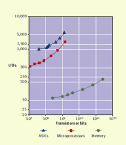 Rent's rule, originally proposed in 1971, indicates a direct relationship between gates, or rather transistors, and I/O. The SIA has extended it in its 1997 National Technology Roadmap for Semiconductors for proposed process technologies through the year 2012, as shown here. |
|
"The basic rule of thumb is to count registers as logic blocks and pick a device that fills only 75 percent with that number of logic elements." But he notes, "This method applies to general types of logic, not highly register-intensive designs, like math elements or highly pipelined datapaths."
Once you know the number of registers, it's easier to pick a device, but you must be sure that the target device has more registers than the design. As well as counting the registers, you need to determine the design's ratio of logic cells to registers. For highly pipelined functions, the number is close to unity. For designs with large percentages of random logic, the estimate is about two to four logic cells per register; the number of flip-flops is between 30 to 60 percent of the design.
To identify the number of gates and registers in a design so that the gate count can be translated into equivalent logic resources in an FPGA, convert the design information into a cell count using the formula:
Cells = ff X n
where ff is the number of flip-flops and n is a design-dependent variable between 1 and 4. Highly pipelined designs and complex multiclock functions like telecommunications circuits will be closer to one logic cell per register, whereas the control logic functions will use close to three logic cells per register.
The definition of a logic cell is fairly vendor-specific, so either use some primitive element like an n-input look-up table or make additional adjustments for the varying number of gate equivalents per basic programmable logic block.
Fitting the I/O into the package
Given the estimated gate count, the designer can apply Rent's rule
to see if the design fits into the desired package. For ASICs and large
programmable devices, Rent's rule indicates that the I/O count is a function
of the number of transistors or bits (calculated from the gate count):
nI/O = k(ng)p
where nI/O is the number of I/Os, k is a process constant, ng is the number of transistors or bits, and p is some fraction between 0.3 and 0.8 that represents functionality and structure. Rent's original values were 3.5 and 0.6 for k and p. For DRAM, though, the values of k and p are much lower than for a similar device count for a microprocessor or an ASIC (see the figure), so the mix of functions in a design will determine the specific values. (Of course, Rent's rule can be used to estimate the gate count, given the number of I/Os.)
One additional correction for ASICs is to account for the extra power, ground, and clock pads by adding a pair of pads for each 100 mA of supply and clock current. This addition will produce a final pad count that matches the device requirements, rather than a count that just addresses the I/Os.
For FPGAs, first determine the pad count and I/O limitations--the number of available pins and the available structure for the pins (input only, output only, or programmable). After determining the number of I/Os, find families of devices that offer the target and the next larger package size, in case the design grows. Finally, estimate the number of registers and calculate logic cell count.
By estimating the total number of logic elements and doubling the count, the designer can then target a device from a programmable logic family. Choosing from a family of devices allows head room for the design to grow as logic is optimized and more functions are added to the design requirements. Note that the value of package migration capabilities within a programmable logic family lies in getting a larger number of logic cells and registers in the same package footprint. As long as the estimated gate count remains below half of the largest device in the family, the design will fit on a single FPGA.
For ASIC designs, the same type of estimates are available. To convert the basic storage element into gates, use 9 to 10 gates per flip-flop. To convert the ratio of logic blocks into registers, use 12 gates per block. The resulting estimate for the design size is the number of registers times 12 gates per register for highly pipelined designs to 36 gates per register for random logic. You must, of course, adjust the total gate count for the number of gates in a register. That value will change depending on the type of clocked storage device--latch, register, scan-based, or the like.
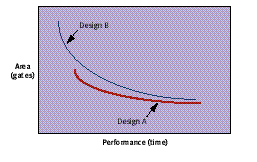
| Synthesis and Banana Curves |
|---|
| Designs vary considerably as they proceed through synthesis. For a
given design, the gate count can move across a fairly wide range. The complex
interactions of the algorithms don't produce linear changes, but instead
operate on a curve (see the figure).
For a single design, the total variance is in the range of 10 to 25 percent of the area. The amount of change varies as a function of the optimization processes. If the design is optimized globally, it will vary about 20 percent in area and 10 percent in speed; if it's optimized on a critical path basis, its area will change about 10 percent, while its speed can range as much as 30 percent. If too many variables are constricted, the range of variation will be very small, since the synthesis will be starting near the high-performance end of the range. In today's design methodologies, only 30 to 80 percent of a design is synthesized. That the entire design isn't synthesized makes the gate estimation process more critical, because the range of variation is reduced even more. If the designer finds that the area/performance curve doesn't achieve the desired results, he or she will start to change the architecture and perhaps some of the constraints. Typically, that occurs in those cases more concerned with performance than area, First, they make a few iterations on Design A until the design seems to come to its limits. Then they change the design by adding resources and pipeline stages to get the desired performance (Design B), thus moving to new curve.
|
An additional refinement, for partially completed FPGA designs, is to factor in the availability of routing resources. This step is important because not all routing resources are equal. The ability to connect directly from one logic block to another without resorting to the global resources improves performance, but it may make other interconnections more difficult.
To consider the routing resources as well, the previous formula becomes Cells = ff X n X R, where R is a number between 0 and 1 that reflects routing and interconnect complexity. For a highly structured design, R will approach 1, whereas for a mass of interfaces and control logic, the value may be closer to 0.5. This number also depends on the size of the logic cells and the need or ability to cross cell boundaries for a logic function.
Synthesis
As the design progresses, you can use a synthesizer's trial synthesis
capabilities for more accurate resource utilization numbers. Many synthesis
tools have a fast mode, especially for RTL designs, that's unconstrained.
When coupled with a generic library that has well-known characteristics,
the tool can provide significant information, not only on size, but on
timing and sometimes power as well. Trial synthesis is faster and more
accurate than guessing the design size when a majority of the design is
completed.
If the trial synthesis indicates that the design is approaching 80 percent of the capacity of any of the resources--logic cells, registers, routing resources--then you must contemplate moving to the next larger device. If this is the largest cost-effective device in a family, then either repartition the design into multiple devices or adjust the design performance in the synthesis tool to reduce the overall design size.
Hardware emulation and acceleration companies also have estimation tools for gate counts for ASICs . One of the issues in emulation is the difference between the hardware implementation and the silicon. The estimate in the emulation software is for emulation gates, which are gates in the emulation reference library. Those aren't the same as "real" ASIC gates. The estimated number of gates is usually within about 10 percent of the final ASIC gate count.
An accurate estimation is also necessary if you're using a hardware accelerator, to ensure that the design fits into the tool. Accelerators use "worker gates"--gates that are transparent to the user but allow probing and assessment of timing parameters within the design. The hardware overhead is a function of the model accuracy. For example, an emulation flip-flop might take 30 to 40 gates if the full timing library is used, but a simplified version will be closer to the ASIC gate count.
To voice an opinion on this or any Integrated System Design article, please email your message to miker@isdmag.com.
[Articles
from Integrated System Design Magazine] [ICs
and uPs]
[Custom ICs and Programmable
Logic] [Vendor
Guide]
[Design and Development
Tools] [Home]