![]()
here.
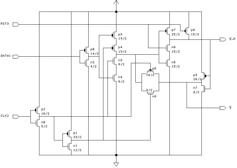
------------------------------------------
CLK	DATA	RST	Q	Q_b
------------------------------------------
1	x	1	Qn-1	Qn-1'
0	0	1	0	1
0	1	1	1	0
x	x	0	0	1
------------------------------------------
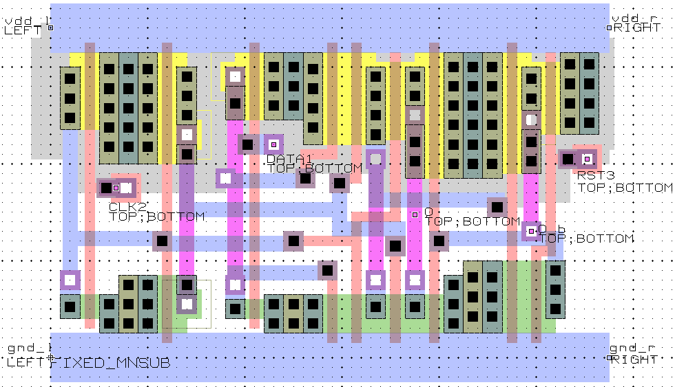
--------------------------------------------
Name	X_loc	Y_loc	   Capacitance (fF)
	lambda  lambda   2U	1.2U	0.8U
--------------------------------------------
CLK2	13.5	35	53.9	24.4	15.6
DATA1	46	44	48.7	22.9	14.7
Q	75	29.5	-	-	-
Q_b	99	26	-	-	-
RST3	110.5	41	71.6	33.8	21.9
--------------------------------------------