![]()
here.
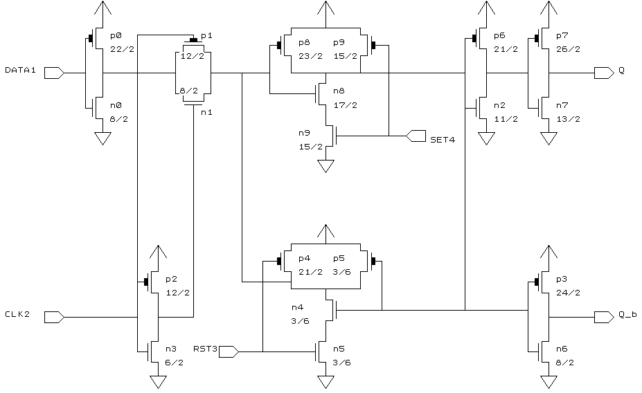
Q_b = Qn'
----------------------------------------------------
CLK	DATA	RST	SET	Q	Q_b
----------------------------------------------------
1	x	1	1	Qn-1	Q_bn-1
0	0	1	1	0	1
0	1	1	1	1	0
x	x	0	1	0	1
x	x	1	0	1	0
----------------------------------------------------
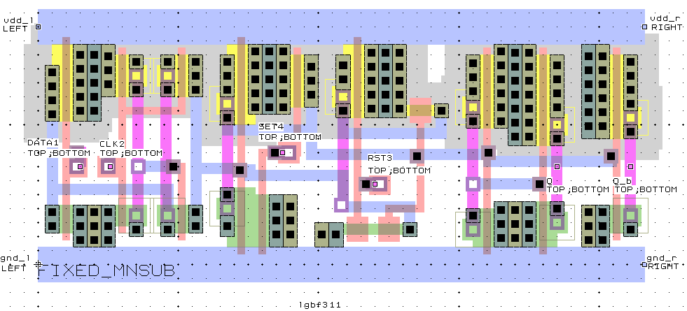
--------------------------------------------
Name	X_loc	Y_loc	   Capacitance (fF)
	lambda  lambda   2U	1.2U	0.8U
--------------------------------------------
CLK2	20.5	28	73.5	53.0	34.1
DATA1	12	28	72.8	57.9	39.7
Q	148	28	-	-	-
Q_b	169	28	-	-	-
RST3	96	23	70.7	52.4	37.9
SET4	69.75	32	78.2	58.6	39.6
--------------------------------------------