![]()
here.
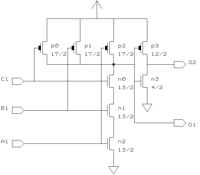
O2 = A1 * B1 * C1
-----------------------------------
A	B	C	O1	O2
-----------------------------------
0	x	x	1	0
x	0	x	1	0
x	x	0	1	0
1	1	1	0	1
-----------------------------------
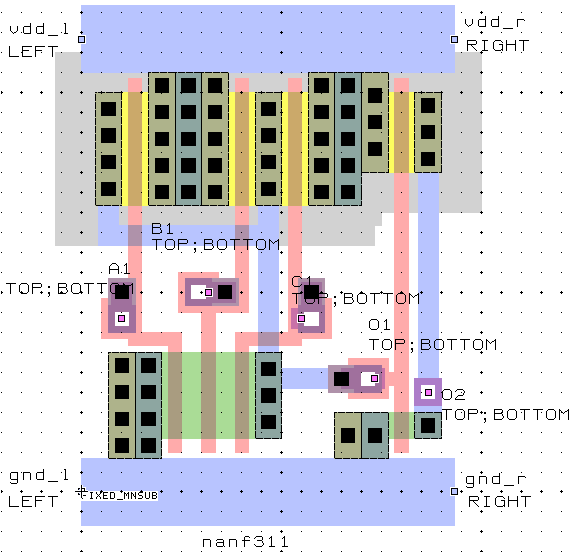
--------------------------------------------
Name	X_loc	Y_loc	   Capacitance (fF)
	lambda  lambda   2U	1.2U	0.8U
--------------------------------------------
A1	6	26	74.8	35.4	23.4
B1	19	30	70.4	33.5	22.2
C1	33	26	67.2	31.8	20.7
O1	44	17	-	-	-
O2	52	15	-	-	-
--------------------------------------------