![]()
here.
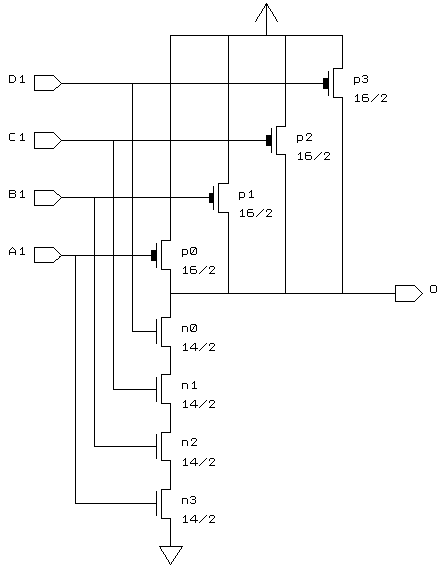
---------------------------------
A	B	C	D	O
---------------------------------
0	x	x	x	1
x	0	x	x	1
x	x	0	x	1
x	x	x	0	1
1	1	1	1	0
---------------------------------
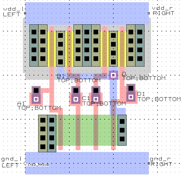
--------------------------------------------
Name	X_loc	Y_loc	   Capacitance (fF)
	lambda  lambda   2U	1.2U	0.8U
--------------------------------------------
A1	5	29	77.1	36.1	23.7
B1	23	29	68.5	32.3	21.5
C1	32	29	66.8	31.8	21.1
D1	48	30	67.1	31.4	20.4
O	40	40	-	-	-
--------------------------------------------