![]()
here.
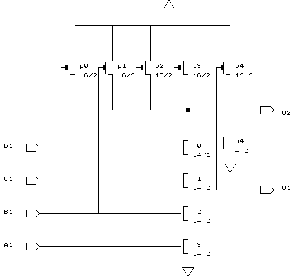
O2 = A1 B1 * C1 * D1
-------------------------------------------
A	B	C	D	O1	O2
-------------------------------------------
0	x	x	x	1	0
x	0	x	x	1	0
x	x	0	x	1	0
x	x	x	0	1	0
1	1	1	1	0	1
-------------------------------------------
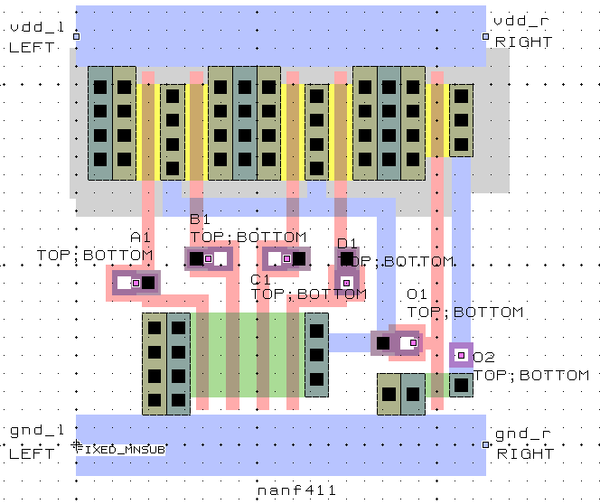
--------------------------------------------
Name	X_loc	Y_loc	   Capacitance (fF)
	lambda  lambda   2U	1.2U	0.8U
--------------------------------------------
A1	10	27	76.7	35.9	23.6
B1	22	31	69.2	32.6	21.7
C1	35	31	67.2	31.8	21.1
D1	45	27	66.3	31.0	20.1
O1	56	17	-	-	-
O2	64	15	-	-	-
--------------------------------------------