Digilab XLä Board Description
·
General Purpose Slide Switches SW1-SW8
·
Push Buttons BTN1-BTN4
· LEDs
·
Seven-Segment Displays
· Clocks
·
Audio Connector
·
PS/2 Connector (J5)
·
Serial Port (J4)
·
Parallel Port (J7)
·
VGA Connector (J6)
·
Power Supply
This write-up gives a brief description of the Digilab XL board to get you started with the laboratory exercises. For more detailed information, please consult the Digilab XL Users Manual on the Digilent, Inc. website, or the references at the back of this document.
The Digilab is a handy board to implement digital circuits on a Xilinx FPGA. The board contains a Spartan XCS10 (5V) or Spartan XCS10XL (3.5V) FPGA. The board also provides 4 seven-segment displays, 8 LEDs, 8 general-purpose switches, four button switches, a serial port, a parallel port, PS/2 mouse and keyboard connector, VGA port, an 1/8” audio connector, a BNC connector, 2 on-board clocks, a ROM, a regulated power supply, a breadboard and several connectors for easy access to the FPGA pins. A simplified schematic of the board is shown in Figure 1 below.
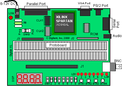
Figure 1: Simplified chematic diagram of the Digilabä board [1]. Only the main components (switches, LEDs, display and connectors) are shown.
General Purpose Slide Switches SW1-SW8
These switches (SW1-SW8) can be used to supply a “1” (Vdd) or a “0” (GND) to the pins of the FPGA. These are single-pole, double-throw switches, shown below. The switches connect both to the FPGA pins and the pins of the J1 connector (see Figure 1) as indicated in the table below. The switch will provide a “1” (Vdd) when the slider is in the down position (towards the edge of the board) and a “0” (GND) when in the up position.
The availability of the signals on connector J1 can be handy to measure the value of the signals or to connect it to the inputs of other components (e.g. placed on the protoboard). A 4.7 KW resistor is put in series with the switch, as shown in the Figure 2 below. The presence of a relatively large resistor of 4.7 KW makes it possible to use the FPGA pins, which are connected to these switches, as outputs instead of inputs. The output buffer of the FPGA can provide enough current to drive these resistors high or low. Alternatively, the FPGA pins can also be driven from an external source through the pins on the J1 connector.
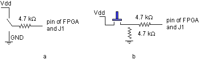
Figure 2: (a) Schematic of the slide switches SW1-SW8; (b) push button switches BTN1-4
Table: Pin connections for the general purpose slide switches
|
Slide Switch # |
Pin # on FPGA |
Pin on J1
Connector |
|
1 |
28 |
SW1 |
|
2 |
27 |
SW2 |
|
3 |
26 |
SW3 |
|
4 |
25 |
SW4 |
|
5 |
24 |
SW5 |
|
6 |
23 |
SW6 |
|
7 |
20 |
SW7 |
|
8 |
19 |
SW8 |
Push Buttons BTN1-BTN4
The Digilab board provides four push buttons which are normally connected to GND (“0”) and which can be momentarily connected to Vdd (“1”). The buttons are connected to both to the FPGA pins and the pins of the J1 connector as indicated in the table below. A 4.7 KW resistor is put in series with the switch, as shown in the Figure 2 what makes it possible to use the FPGA pins as outputs.
|
Push Button # |
Pin # on FPGA |
Pin on J1
Connector |
|
1 |
59 |
BTN1 |
|
2 |
58 |
BTN2 |
|
3 |
57 |
BTN3 |
|
4 |
56 |
BTN4 |
LEDs
Eight LEDs are provided to display the value of output signals. The LED will light up when a “1” (Vdd) is applied to its input (anode) and will be off when a “0” (0V, low or GND) is applied. The signals can come both from the FPGA or from the pins on the J1 connector, as shown in the table below. One should be careful not to drive the LEDs from both the FPGA and the J1 connector.
|
|
LED drive signal
LD |
Gate Signal LDG |
||
|
LED# |
Pin # on FPGA |
Pin J1 |
Pin # on FPGA |
Pin J1 |
|
1 |
69 |
LD1 |
70 |
LDG |
|
2 |
68 |
LD2 |
||
|
3 |
67 |
LD3 |
||
|
4 |
66 |
LD4 |
||
|
5 |
65 |
LD5 |
||
|
6 |
62 |
LD6 |
||
|
7 |
61 |
LD7 |
||
|
8 |
60 |
LD8 |
||
An tri-state octal D-type latch (74HC373) is used between the LEDs and the pins from the FPGA or the J1 connector as shown in Figure 3. This latch has a latch-enable input (LDG) that has to be HIGH for the output to follow the input D. When the LDG input is LOW, the output will retain its original value This makes it possible to use the pins of the FPGA, which are connected to the LED), for other purposes as well. The latch-enable (gate signal) LDG signal (common to all 8 registers) can be driven from the FPGA or the J1 connector, as indicated in the table above. The output-enable control input is always connected to GND, in order to keep the outputs enabled all the time.
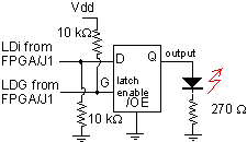
Figure 3: Connection of the LEDs (after [1])
Seven-Segment Displays
The Digilab provides four seven-segment displays that can be used to display data from the FPGA or from other circuits through the J1 connector. The segments of each display are called A, B, up to G as is shown in Figure 4a below. In order to reduce the number of connections needed to address each of the LEDs (Light Emitted Diode), the anodes of the LEDs of each seven-segment display have been connected together. The common anode for the first seven-segment display is called A1, A2 for the second display, etc. In addition, the cathode pins from each display have been connected together to form seven common terminals, called A, B, C, D, E, F and G, corresponding to the seven-segments (see Figure 4b and c). Thus to illuminate a segment of a particular display, e.g. segment E of the third display, one has to apply a “1” (High or Vdd) to anode A3 and a “0” (GND or Low) to cathode node E. In addition to the seven segment LED, there is also a decimal point available (DP). However, the decimal point is not connected to the FPGA but to a pin of the J1 connector. If one needs to drive the decimal point, one can use a general purpose output of the FPGA and connect this output to the DP pin on the J1 connector.
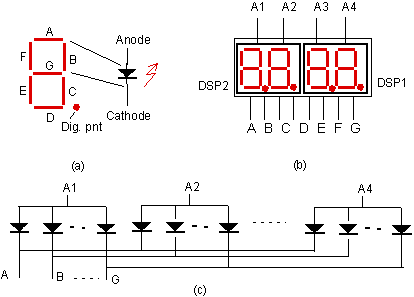
Figure 4: Seven-segment display: (a) Seven-segment display; (b) four displays with common anode; (c) LED connections
The table below shows the pin numbers on the FPGA corresponding to the anode
and cathode terminals.
Table: Four seven-segment display pin connections
|
Seven-segment Terminal |
Pin # of FPGA |
Pin on J1 connector |
|
A1 (Anode digit 1) |
44 |
A1 |
|
A2 (Anode digit 2) |
40 |
A2 |
|
A3 (Anode digit 3) |
39 |
A3 |
|
A4 (Anode digit 3) |
38 |
A4 |
|
A (Cathode of segment A) |
51 |
CA |
|
B |
50 |
CB |
|
C |
49 |
CC |
|
D |
48 |
CD |
|
E |
47 |
CE |
|
F |
46 |
CF |
|
G |
45 |
CG |
|
Dec. point |
- |
DP |
Clocks
The Digilab board has two clocks, CLK1 and CLK2. The CLK1 clock is the general system clock that has been connected to pin 13 (PGCK1)of the FPGA. It provided a clock of 25.175MHz. CLK2 is connected to pin 35 (PGCK2) of the FPGA as well as to pin CLK2 on the J1 connector. The second clock can come in handy for peripheral devices which need a clock.
|
Clock |
Pin # on FPGA |
Pin on J1 connector |
|
CLK1 (25.175 MHz) |
13 (PGCK1) |
- |
|
CLK2 |
35 (PGCK2) |
CLK2 |
The Spartan XS FPGA has also an on-chip oscillator that runs nominally at 8Mz and can be divided down to 500 kHz, 16 kHz, 490 Hz and 15 Hz. The on-chip oscillator is used by placing the OSC4 component in the schematic or HDL code.
BNC Connector
The BNC connector can be used to supply or measure a high frequency signal. The middle wire (post) carries the signal while the outer wire is the shield that is usually connected to the GND (not connected on board). The connections are shown in the table below. To connect the BNC to a pin of the FPGA one can use a jumper between the pins on the J1 connector.
BNC Connector |
J1 Connector |
|
Post (inner conductor) |
BNCP |
|
Shield (outer conductor) |
BNCS |
Audio Connector
The 1/8” audio connector can be used for a speaker or microphone connection. Both channels are connected together to a common ASFT signal, shown in Figure 5. The ASFT and the ATIP signals are connected to the pins of the J1 connector
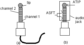
Figure 5: Audio connector: (a) audio plug; (b) plug and audio jack
|
Audio Connector |
J1 Connector |
|
Tip |
ATIP |
|
Channel 1 |
ASFT |
|
Channel 2 |
PS/2 Connector (J5)
The PS/2 connector can be used for a mouse or keyboard. The pin numbering is shown in Figure 6 and the table below. The Data and Clock signals are connected to connector J2 and the pins of the FPGA.
|
PS/2 Pin |
Function |
Pin # on FPGA |
J2 connector |
|
1 |
Data |
83 |
PS2D |
|
2 |
Reserved |
- |
- |
|
3 |
GND |
1,12,21,31,43,52,64,76 |
GND |
|
4 |
Vdd |
2.11,22,33,42,54,63,74 |
|
|
5 |
Clock |
82 |
PS2C |
|
6 |
Reserved |
- |
- |
|
|
|
|
|
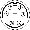
Figure 6: PS/2 connector –front view.
Serial Port (J4)
The serial port can be used for serial transmission of signals. The RS-232 standard specifies the voltage levels [4]. A RS-232 voltage converter (Maxim MAX202) has been added to the board to convert to the right voltage levels. The serial port makes use of a 9-pin DB9 connector whose pin numbers and function are given in the table below. The serial port implemented on the Digilab board allows two-wire communications, using the RXD and TXD signals (routed to the FPGA and J2 connector). The TRS and CTS signals are not routed from the Maxim voltage convertor to the FPGA or any of the connectors.
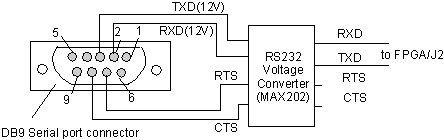
Figure 7: Serial port connector – front view
|
Serial Port Pin |
Name |
Function |
Pin # FPGA |
Pin on J2 |
|
1 |
DTR |
Data terminal ready |
- |
- |
|
2 |
RXD |
Received Data |
72 |
RXD |
|
3 |
TXD |
Transmitted Data |
75 |
TXD |
|
4 |
DCD |
Data carrier detect |
- |
|
|
5 |
SG |
Signal ground |
- |
|
|
6 |
DSR |
Data set ready |
- |
|
|
7 |
CTS |
Clear to send |
- |
|
|
8 |
RTS |
Request to send |
- |
- |
|
9 |
RI |
Ring indicator |
- |
- |
Parallel Port (J7)
The parallel port can be used for two purposes: data communication and for programming he FPGA. The choice between the two modes are set by setting switch SW9 in the “PORT” (for parallel data communication) or in the “PROG” (programming) position.
a. Parallel data communication
The pin numbers of the DB25 parallel port connector, used for data communication, are given in the table below. The names of the Enhanced Parallel Port (EPP) mode are used in the table but any other protocol can be implemented for data transfer.
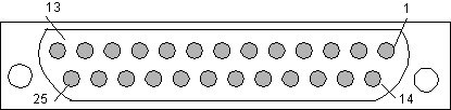
Figure 8: DB25 parallel port connector – front view
|
Pin |
EPP signal |
EPP Function |
Pin FPGA |
Pin J1 & J3 |
|
1 |
Write enable (O) |
Low: read; High: write |
3 |
PWE |
|
2-9 |
Data line PD0 |
Bi-directional Data line |
4 |
PD0 |
|
3 |
Data line PD1 |
Bi-directional Data line |
5 |
PD1 |
|
4 |
Data line PD2 |
Bi-directional Data line |
6 |
PD2 |
|
5 |
Data line PD3 |
Bi-directional Data line |
7 |
PD3 |
|
6 |
Data line PD4 |
Bi-directional Data line |
8 |
PD4 |
|
7 |
Data line PD5 |
Bi-directional Data line |
16 |
PD5 |
|
8 |
Data line PD6 |
Bi-directional Data line |
18 |
PD6 |
|
9 |
Data line PD7 |
Bi-directional Data line |
17 |
PD7 |
|
10 |
Interrupt (I) |
Interrupt or Acknowledge input |
84 |
PINT |
|
11 |
Wait (I) |
Bus handshake; low to acknowledge |
15 |
PWT |
|
12 |
Spare |
Not connected |
|
|
|
13 |
Spare |
Not connected |
|
|
|
14 |
Data Strobe (O) |
Low when data valid |
14 |
PDS |
|
15 |
Spare |
Not connected |
|
|
|
16 |
Reset (O) |
Low to reset |
10 |
PRS (J3 only) |
|
17 |
Address Strobe (O) |
Low when address valid |
9 |
PAS |
|
18-25 |
GND |
ground |
|
GND |
b. Programming mode
The parallel port can be used to program the FPGA. Make sure that switch SW9 is in the “PROG” position. The Xilinx Project Manager will automatically detect the parallel cable and enable programming over this port. In case the cable is not automatically detected one can manually set the cable type in the Hardware Debugger Window: from the Cable pull down menu, select Communications; in the communications set up window: select Parallel).
When programming the FPGA through the parallel port one
should make sure that one does not apply data signals to the ports until one
has placed the switch SW9 in the “PORT” position.
When programming the FPGA from the on board ROM, one should place switch SW9 in the “PORT” position. Programming will start as soon as one power on the board.
VGA Connector (J6)
A DB15 connector (Figure 9) is used for the VGA signals. The 5 signals are available on the pins of the FPGA and the J2 header. The signals are terminated with a 75 W pull-down resistor. The Read, Green and Blue signal lines have a series resistor of 470 W inserted between the pins of the DB15 connector and the FPGA and J2 connector.
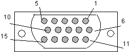
Figure 9: VGA connector – front view
Table: VGA Connector (DB15)
|
DB15 VGA pin no. |
Name |
Pin # on FPGA |
J2 connector |
|
1 |
R (Red) |
77 |
R |
|
2 |
G (Green) |
78 |
G |
|
3 |
B (Blue) |
79 |
B |
|
6,7,8,10 |
GND |
|
GND |
|
13 |
Hor. Sync. |
80 |
HS |
|
14 |
Vert. Sync. |
81 |
VS |
|
12,4,9,5,15 |
Not connected |
- |
- |
Power Supply
The Digilab XL comes with an on-board voltage regulator (LM317T) that can be set to deliver 5V or 3.3V. By selecting the proper value of the resistor R6 one can produce 3.3V (R6=390W) or 5V (R6= 750W). The XCS10XL requires a 3.3V while the SCS10 requires a 5V supply. An AC adaptor (supplied with the board) that outputs a 6-12V DC voltage provides power to the regulator, through jack J8. When the board is power up the LED LD9 will light up.
References
- Digilab XL Users Manual, Digilent, Inc. Pullman, WA (http://www.digilent.cc/XLAusersmanual.pdf ) or the Digilent website (http://www.digilent.cc/)
- Xilinx Databooks: Spartan and Spartan XL FPGA data sheet, Xilinx, Inc, 2000.
- 74HC373 Tri-State Octal D-Latch, Fairchild Semiconductor Corp, 2001: http://www.fairchildsemi.com/pf/MM/MM74HC373.html
- P. Horowitz and W. Hill, “The Art of Electronics”, Cambridge University Press, New York, 1989.
Created by Jan Van der Spiegel July 5, 2001; updated January 25, 2002.