The ability to model varying signal levels as produced by digital hardware is fundamentally important for the simulation of switch level circuits. This is accomplished by assigning various signal strengths as defined in Table 1. The signal strengths vary from supply level own to high impedence level, covering six distinct intermediate levels. Each level can represent a logic 1 (supply1, strong 1 ..... highz1) or a logic 0 (supply0, strong0 ..... highz0).
Strength Name |
Strength Level |
Element Modelled |
Declaration Abbreviation |
|
Supply Drive |
7 |
Power supply connections. |
supply |
|
Strong Drive |
6 |
Default gate & assign output strength. |
strong |
|
Pull Drive |
5 |
Gate & assign output strength. |
pull |
|
Large Capacitor |
4 |
Size of trireg net capacitor. |
large |
|
Weak Capacitor |
3 |
Gate & assign output strength. |
weak |
|
Medium Capacitor |
2 |
Size of trireg net capacitor. |
medium |
|
Small Capacitor |
1 |
Size of trireg net capacitor. |
small |
|
High Impedence |
0 |
Not Applicable. |
highz |
Signal strengths are used by the Verilog simulator in two main situations : modelling of weak (resistive) transistors and resolving signal contention.
Return to : the document top or the section top.
Weak or resistive transistors have many uses within the domain of digital design. A property associated with resistive transistors is that any signal passed through one is degraded. This is modelled within Verilog using signal strengths which are reduced when they encounter resistive transistors. Signals are degraded as indicated in Table 2.
Input Strength |
Output Strength |
|
supply |
pull |
|
strong |
pull |
|
pull |
weak |
|
weak |
medium |
|
large |
medium |
|
medium |
small |
|
small |
small |
|
highz |
highz |
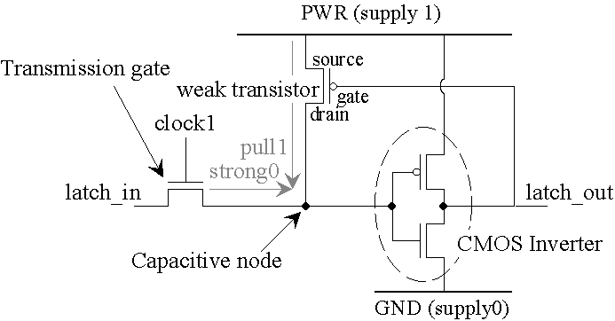
One such occasion where this technique is needed is for the digital latch (Figure 1), where a weak transistor is used to reinforce the poor logic 1 passed by the transmission gate. The logic 1 imposed by this weak transistor can however be overcome by the strong logic 0 passed by the transmission gate.
Figure 1 : simple latch circuit exhibiting signal contention.
Return to : the document top or the section top.
The situation often arises whereby two signals drive one node in a circuit resulting in signal contention (Figure 2). The strength and logic value of the two signals are used to resolve the signal conflict to produce a single logic value and strength on the node.
Three situations can arise.
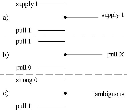
Figure 2 : a) Similar logic, strength contention.
b) Similar strength, logic contention.
c) Logic and strength contention.
Return to : the document top or the section top.
Any problems or queries email :
S.I.Penman@ug.ee.ed.ac.uk