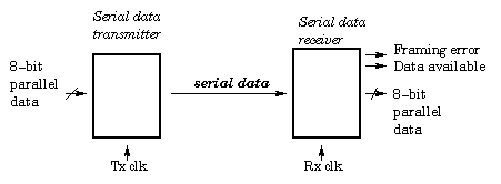
The above figure shows a simplified picture of an asynchronous serial interface of the type commonly used to transfer data in computer and communications systems. The data transfer is referred to as `asynchronous' because the spacing between the characters may be of any length. In contrast, the timing of the bits within the character is well defined (and is related to the baud rate of the interface). The Tx clock and Rx clock signals are nominally of the same frequency, but are generated locally at each end of the transmission link and therefore cannot be assumed to be `locked' together. The design of a suitable transmitter circuit is not difficult, but the receiver must be able to detect the start of an incoming character and then store the value of each data bit, despite the fact that the relative frequency and phase of the Tx and Rx clocks may vary.
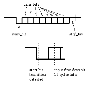
As shown in the data diagram, the beginning and end of each character is delimited by a start bit whose value is always 0, and a stop bit whose value is always 1. In between characters, the transmitter outputs a constant value of 1. In operation, the receiver continually samples the input data. Following a 1 -> 0 data input transition, the eight data bits must be stored, and this is where a problem may occur, since for maximum reliability we wish to sample the data bits in the centre of their bit times and not close to either edge, so that small differences between the Tx and Rx clocks can be accommodated. This may be accomplished by using an Rx clock frequency which is a multiple of the data bit rate. In this exercise we shall assume that the Rx clock signal is eight times the bit rate.
Following the detection of a start bit, the stop bit should be detected 76 clock cycles later. If so, the Data Available output is set high; if not, the Framing Error output is set. Both status outputs are reset low by the detection of the next start bit.
There is thought to be a danger of spikes on the communication channel falsely starting the receiver. This means that a momentary LOW on the input to the receiver would be seen as a one-to-zero transition where-as it is really just noise.
To counter this, the specification is changed as follows:
Thus you will have to update your design for detectng a valid start bit.
Note:- the flexibility of 3-4-5 clock periods is to allow you to implement whichever is simplest - BUT there is no definition of what value is on the input at the sample AFTER the one-to-zero transition: this is to avoid problems associated with signal bounce.
You are STRONGly advised to try to implement this using a purely synchronous design style.
Consider the major submodules which make up the design BEFORE reading any further.
and when you have a good idea as to how it should be done,
then take a look at my
suggestion.