Low-power double-edge triggered flipflops are presented using weak feedback transistors which allow purely n-type transmission gates but without static-power consumption. The switching capacitance of the weak transistors is minimized by using permanently ON transistors in series as resistive devices. Both static and semi-static circuits are presented.
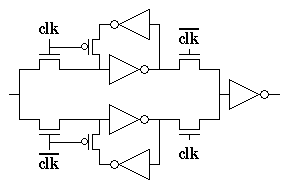
Double edge-triggered flipflops are becoming a popular technique for low-power designs since they effectively enable a halving of the clock frequency. The paper by Hossain et al[1] showed that while a single-edge triggered flipflop can be implemented by two transparent latches in series, a double edge-triggered flipflop can be implemented by two transparent latches in parallel; the circuit in Fig. 1 was given for the static flipflop implementation. The clock signal is assumed to be inverted locally. In high noise or low-voltage environments, Hossain et al noted that the p-type pass-transistors may be replaced by n-types or that all pass-transistors may be replaced by transmission gates.
This letter will show that weak feedback transistors with resistive loads can reduce power consumption in this circuit leading to a design with lower power consumption that other reported circuits.
The circuit in Fig. 1 suffers from sub-threshold currents due to the threshold voltage drop across the pass transistors. These can be eliminated using full transmission gates; however this raises the number of transistors which switch with the clock signal from 8 to 14.
Instead, we propose the circuit shown in Fig. 2 - using only 6 transistors which switch with the clock. The transistor and inverters marked with *s are weak to allow the nodes they drive to be switched by other outputs. This necessitates careful ratioing of the transistor sizes and verification of the chosen sizes over all fabrication conditions.
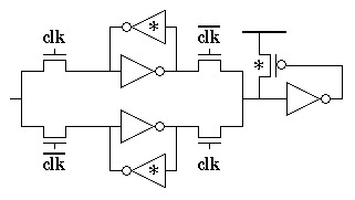
The feedback inverters perform two functions: first, the pullup transistors restore the logic-high voltage level following the threshold voltage drop of the n-type pass-transistor; second, the pulldown (with the pullup) transistors lead to a fully static configuration when the latch is non-transparent. Clearly further power savings are possible if this is not required. The final feedback circuit, however, only requires a p-type pullup since if the inverter input is low it will be connected to ground through the non-transparent latch.
The main disadvantage is that weak transistors are generally formed using long, and so high capacitance, gates; however, Farnsworth et al[2] suggest using additional transistors in series, which are permanently ON, to act as load devices - this is illustrated in Fig. 3 for an inverter. The advantage is that the gate capacitance is the same as that of a minimum-area inverter while the length of the combined series transistors can be optimized independently. The derivation of the sizes shown in Fig. 3 is described below.
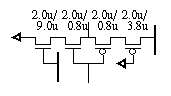
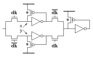
Fig. 4 shows the circuit which results from removing the n-type pulldown transistors in the feedback circuits: this is only semi-static in that the nodes x and y isolated when low. However, these nodes only becomes isolated when the gate of the preceding pass-transistor is lowered, and so any cross-coupling capacitance between the transistors gate and source/drain will reduce rather than raise the corresponding node's voltage level; each node is only isolated for half the clock period.
The key point in both the static and semi-static circuits is that the weak p-type feedback transistors allow the use of purely n-type transmission gates without the penalty of static-power consumption due to the threshold voltage drop. The proposed designs thus have fewer transistors driven by the clock signal which accounts for the reduction in overall power consumption.
Circuit level simulations were conducted using HSPICE with level 6 parameters for ES2-Atmel's ECPD07 process at 5V and typical conditions. Several input vectors were used. B and C are constant inputs (high and low respectively); D and E have input changes on every and every-other clock phase; F is a constant output but with an input glitch on every clock phase (0->1->0); and A is an amalgam of all the above formed by one event of both high and low type on both clock phases.
Except for the weak inverters as described above, "minimum area" transistor sizes are used: W=2u, L=0.8u. The transistor sizes in Fig. 3 were chosen by varying the lengths of the ON transistors to minimize power consumption for vectors A. The 2u/9u transistor may be implemented with a smaller area using the equivalent ratio of 1u/4.5u. The proposed circuits were simulated at the four process corners to ensure correct operation over process spread.
Fig. 5 shows the average power consumption using typical conditions and a 50MHz clock for the circuits: 1) Fig. 1, 2) Fig. 1 with transmission gates, 3) Fig. 2, and 4) Fig. 4. In each case, the inverse clock is generated by an inverter, and the input signals are driven by inverters so that the effects of input capacitance are included in the power measurement.
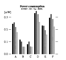
The effect of static-power consumption on the Fig. 1 circuit can be seen in the different total-power consumption between a constant high (B) and a constant low (C) input. This effect, and the relatively high power-consumption of this circuit, were far more marked in simulations with lower clock frequencies: at 5MHz the power-consumption of Fig. 1 is more than double that of Fig. 2 for four out of the six simulation vectors.
In comparison to the use of transmission gates to eliminate static power consumption, the proposed circuits use less power with all simulation vectors; for instance, when the inputs to the flipflops do not change there is a 38% power reduction.
We have shown the circuit design of a static and semi-static double-edged triggered flipflop. By using permanently ON transistors in the feedback circuits, we avoid the penalty of extra capacitance associated with sizing the transistors to make them weak. Further the feedback p-type transistor connected to the inputs of the standard inverters allows the use of only n-type, and fewer, transistors in the transmission gates driven by the clock signal. Together, these circuit techniques enable a lower power consumption than the original designs.
The author is a senior lecturer at
The Department of Electrical Engineering, The University of Edinburgh
The King's Buildings, Edinburgh, EH9 3JL, Scotland, UK