![]()
|
|
![]()
Leopard leaps into structured ASICs
By Ron Wilson, EE Times
January 26, 2004 (11:18 AM EST)
URL: http://www.eetimes.com/article/showArticle.jhtml?articleId=18310559&sub_taxonomyID=6257
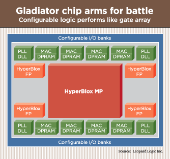
San Mateo, Calif. - Leopard Logic Inc. (Cupertino, Calif.), which earlier had cast itself as an intellectual-property company, this week will introduce a line of chips to attack the structured-ASIC market. By combining a large via-mask-configurable logic fabric with smaller regions of SRAM-configured field-programmable logic, embedded memories and embedded multiply-accumulator blocks, the company hopes to establish its Gladiator configurable logic device (CLD) family as denser, faster and less expensive than FPGAs but more flexible than structured ASICs.
Leopard (http://www.leopardlogic.com/) is counting on its combination of mask-configured and SRAM-configured blocks to give it a unique position in the market. The mask-configured fabric, like the logic fabric in other structured-ASIC offerings, has interconnect impedance more similar to that of gate arrays. So logic implemented in the fabric can have performance similar to gate-array implementations. Leopard vice president of sales and marketing Stefan Tamme said that typical operating frequencies for subsystems in the mask-configured fabric would be 200 to 300 MHz, and machines limited to one to two layers of logic could operate locally at up to 500 MHz.
The presence of Leopard's FPGA fabric on a die means that significant portions of a design can be implemented in field-programmable logic. Hence, a single chip can combine gate-arraylike density and performance with field programmability, Tamme said. "Typically, functions such as data paths and CPUs would go in the mask-configured fabric. Functions more subject to change, such as control logic for protocol engines or I/O controllers, would go in the field-configurable blocks," he said.
The first device in the family will offer a 64k fabric of via-configurable logic cells, 4k of SRAM-configurable logic cells, just over 2 Mbits of embedded SRAM and 64 MACs. That would give the device a capacity near the high end of current FPGAs. The device is projected to be in about the middle of Leopard's eventual product line in terms of capacity.
Structurally, the device comprises a single large fabric of mask-programmable logic cells, with four smaller blocks of SRAM-configured fabric and 64 embedded MAC/memory blocks embedded within it. The chip has fairly typical configurable I/O cells but does not support LVDS and has no internal serializer/deserializer blocks.
Perhaps the most important architectural element is the way the fabrics are connected. "The I/O architecture between the FPGA fabric and the rest of the chip is the No. 1 place where mixed architectures break down," said Chris Phillips, Leopard's president and CEO. "If you attempt to connect the fabric to the rest of the chip through something resembling an I/O pad ring, you will run out of interconnect."
Instead, Leopard has implemented a proprietary dual-mesh fabric that overlays the chip. One mesh serves internal connections and the other serves connections between regions of the chip, but both provide rich resources accessible to any logic element. Thus when a design requires hundreds or thousands of interconnections between field-configurable and mask-configurable fabrics, the architecture can support the need.
At a microarchitectural level, the chip design rests on two fundamental developments from Leopard's previous FPGA IP product. One is the logic cell, which combines a four-input lookup table (LUT) with a flip-flop. "The 4-LUT is the fundamental element in both Altera and Xilinx logic cells," Phillips said. "But we have extended the normal 4-LUT cell design so that it easily handles up to eight inputs. This greatly improves the efficiency of the fabric for wide-word operations."
Mux-based interconnect
The other development is Leopard's multiplexer-based interconnect scheme. Rather than use a planar arrangement of metal segments connected by pass transistors, Leopard bases its scheme on muxes in a bid to provide superior interconnect performance and connectivity.
The approach also evolved into a single-mask configuration scheme for the mask-configured fabric. The interconnect architecture lent itself to bringing all connection points up to a single via layer, so that all customer-specific connections could be made by either putting in or leaving out vias at predefined sites. That simplifies Leopard's task in turning a base wafer into a customer-specific one. The customer logic gets mapped onto the logic array, the correct via mask is created and the wafers are completed from that layer up.
The base wafers are made at Taiwan Semiconductor Manufacturing Co. Ltd. using a 130-nanometer process. Leopard quotes a four-week turnaround, for a nonrecurring expense of approximately $50,000 (including 10 sample chips).
The architecture fits into a pattern of recent moves in the structured-ASIC area. Early designs, such as those from AMI Semiconductor and NEC, used multiple metal and via layers to customize the chips. But architectures from eASIC Corp., ViASIC Inc. and now Leopard bring all the user connections to a single via layer, so that there is only one customer-specific mask. As eASIC has already demonstrated, this layer doesn't even require a mask - it can be written directly to a wafer by e-beam in a production flow.
Leopard's choice of logic cell is similar in concept to eASIC's. Both companies use SRAM-based LUTs as their fundamental logic element - like the cells used in FPGAs, but quite different from the networks of gates or muxes used in other structured-ASIC designs. But unlike the eASIC fabric, in which each individual cell can be configured as a via-programmed, SRAM-programmed or memory cell, the Leopard architecture provides fixed blocks of each kind of resource.
Leopard hopes to mitigate the inherent granularity of the architecture in two ways. First, a family is in the plans, with devices reaching from 6k logic cells to 272k cells.
Second, all the logic cells are identical, whether they lie in a region of mask-configured or SRAM-configured interconnect. So the tool flow can remain uniform for blocks headed for either kind of fabric. Nor are there hard boundaries between the blocks that would require explicit partitioning and mapping decisions by the design team.
![]()
|
|
|
|