![]()
작성일: 2005.11.14


November 07, 2005
Building an FPGA FIFO without using logic resources
This "How To" article describes how to build a full-featured FIFO in an FPGA without consuming valuable logic resources.
Today, FPGA designers are using these flexible devices to perform everything from simple glue logic tasks to implementing complicated system on a chip (SoC) functions. The efficiency and ease of implementation of these designs are greatly enhanced by the feature-rich embedded elements present in the target technology. While simple FPGAs offer the ability to implement only basic logic functions, more advanced FPGAs provide embedded RAMs, multipliers, and highly specialized IO structures. These embedded elements are building blocks that - when combined with surrounding logic - can turn an embedded RAM into a FIFO, or an embedded multiplier into a finite impulse response (FIR) filter.
Thus, to expand upon these embedded building blocks to create more advanced functions, extra logic must typically be utilized and configured by the designer. This extra logic, in most cases, must be created, verified, implemented, and properly connected to the embedded elements by the designer in the source RTL.
But, what if this weren't the case? What if a designer could simply configure, for example, a highly flexible embedded RAM block in an FPGA to be a FIFO? And, what if this FIFO could have various depths and widths, have programmable output flags, and simultaneously operate in two separate clock domains - all without consuming any additional FPGA logic? Finally, what if this could be done without writing one line of RTL code? All of this is now possible using QuickLogic's new PolarPro line of low-power FPGAs. This paper will discuss how to use the PolarPro device - along with its associated design software, QuickWorks - to build these highly flexible FIFOs without using any of the FPGA's logic resources.
The PolarPro FPGA
Consider the layout of the
QuickLogic PolarPro FPGA (Fig. 1). As can be seen in
the figure, the device has embedded RAM blocks as well as
embedded FIFO controllers.
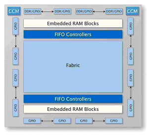
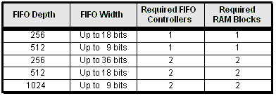
Both of these functions are implemented as hard-wired standard cell (ASIC) gates; however, their functionality is quite flexible. Each RAM block contains 4608 bits of storage, and even in the smallest PolarPro device there are 8 of these RAM blocks. Likewise, for each of the RAM blocks there is a corresponding FIFO controller. The various FIFO configurations are shown in Table 1.
Any mixture of these FIFO configurations can be implemented in a PolarPro device using multiple instances, so long as the total number of RAM blocks and FIFO controllers are not exceeded for the given device.
The following features are available for each of the possible FIFO configurations shown in Table 1 above:
- Asynchronous input and output ports (these ports can be clocked at completely different frequencies).
- Almost empty and almost full output flags.
- Level indicator flag vectors for both the input and output side of the FIFO.
- Data flush inputs for both the input and output side of the FIFO.
- For FIFOs utilizing one RAM block, programmable aspect ratios of 256x18 or 512x9 are independently configurable on the input and output ports.
- For FIFOs utilizing two RAM blocks, programmable aspect ratios of 256x36, 512x18, or 1024x9 are independently configurable on the input and output ports.
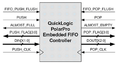
Consider a more detailed view of the PolarPro FIFO controller along with its input and output signals (Fig 2).
FIFO Design
Imagine for a moment if you, as a
designer, were given the task to create a FIFO in an FPGA
using logic resources and embedded RAM blocks. In the case of
a rudimentary implementation, this task is simple enough. All
the designer must do is design the counters and control logic
that feed the address and control inputs for the read and
write side of the RAM blocks. This could be achieved with
minimal logic utilization and the design would be fairly
simple.
Now consider a slightly more complex scenario where the FIFO is also required to output almost empty/full flags and/or output vectors indicating the number of elements that are present in the FIFO. In this case, a subtractor must be implemented in the design between the read and write address counters such that a "fill level" indication of the FIFO can be computed. Once again, this requirement is not unduly difficult to achieve and it can be managed easily in a modest amount of FPGA logic resources.
However, what if we now add the requirement of asynchronous operation in which the input and output ports of the FIFO are clocked at completely different frequencies. In this case, the design becomes much more complicated and consumes much more logic. And if we further add a requirement that the FIFO must have a configurable aspect ration (depth versus width) for the input port versus the output port, the design task now becomes very daunting.
Today's designers are concerned about issues and complex problems that go way beyond how to implement a complex asynchronous configurable FIFO in an FPGA. In fact, most FPGA designers also have many board and system level issues to worry about on any given project. So, it does not make sense to burden designers with having to create this type of RTL design from scratch or even attempting to acquire a completed IP design from a third party to perform this function. Why reinvent the wheel, and why waste valuable FPGA logic resources on such functions when those resources could be better utilized for other truly custom logic applications?
The ideal approach would be if designers could simply enter the parameters for a required FIFO into an intelligent GUI tool, and have this tool output the resultant RTL. The tool should also generate simulation test benches along with a wrapper to easily instantiate the entire finished block into the top level FPGA design without consuming precious FPGA logic resources.
How-to use the QuickWorks PolarPro FIFO wizard
In
order to generate the RTL wrappers and testbenches that enable
the PolarPro embedded FIFO blocks to operate in a given
design, the FIFO Wizard in QuickLogic's QuickWorks design
software is used. The following steps detail how this is
achieved:
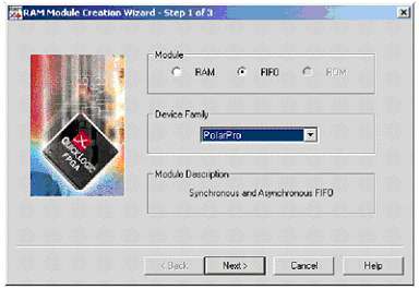
Step 1: From the QuickWorks tool, the FIFO Wizard is launched. The designer selects the FIFO option for the module type and indicates that the target device technology is PolarPro (Fig 3).
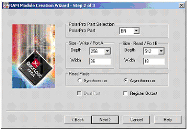
Step 2: Next, the specific device in the PolarPro family is selected, and the required width and depth of the input and output ports on the FIFO are indicated. Furthermore, it is indicated if the input and output ports of the FIFO are to be driven by one clock (synchronously) or by two clocks (asynchronously) (Fig 4).
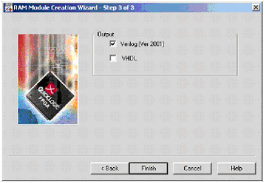
Step 3: Now, the output language is selected (Verilog or VHDL) (Fig 5).
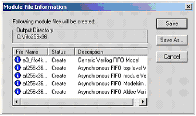
Step 4: Finally, the Wizard ends by indicating the output directory and detailing the files that will be saved (Fig 6).
After completing these four steps, the wrapper RTL and testbenches are automatically generated for the FIFO that the designer has specified in the GUI. These files can be instantiated in the designer's top level FPGA design and will automatically be used to properly configure the embedded FIFO and RAM blocks in the PolarPro device during the FPGA place and route stage. Once these design files have been properly instantiated by the designer into the RTL, the FIFO portion of the design is complete and no further coding or tweaking is required.
Conclusion
The QuickWorks design software allows
designers to effectively utilize the advanced embedded RAM and
FIFO features present in QuickLogic's newest low-power FPGA:
the PolarPro. This combination allows designers to implement
complex FIFOs in an FPGA design using a simple step by step
Wizard as shown in the how-to section of this paper.
The PolarPro FPGA goes beyond providing simple embedded building blocks such as RAM modules; in conjunction with the QuickWorks software, the PolarPro provides a quick and easy method to implement complex FIFOs without consuming any programmable logic resources. As a result, designers can use the available logic in the FPGA for more important custom tasks, and can spend their time designing these application critical functions rather than worrying about how to implement the relatively trivial, yet still complicated design of an asynchronous FIFO.
Being able to access and configure these advanced embedded functions in the FPGA quickly results in lower costs for the overall logic design and a shortened time to market cycle. These features, along with PolarPro's dominant low power position in the FPGA landscape, make this device a very compelling solution for today's system designers.
About the author Judd
E. Heape is Director of Product Applications for
QuickLogic Corporation in Sunnyvale, California. He has been
in the industry for over 14 years (at QuickLogic and
previously at Texas Instruments) and has four granted US
Patents (others pending) and has authored one worldwide JEDEC
standard. Judd holds a degree in Electrical Engineering from
the Georgia Institute of Technology. Judd can be reached at
mailto:judd@quicklogic.com.
Judd
E. Heape is Director of Product Applications for
QuickLogic Corporation in Sunnyvale, California. He has been
in the industry for over 14 years (at QuickLogic and
previously at Texas Instruments) and has four granted US
Patents (others pending) and has authored one worldwide JEDEC
standard. Judd holds a degree in Electrical Engineering from
the Georgia Institute of Technology. Judd can be reached at
mailto:judd@quicklogic.com.
![]()
![]() Send to a colleague |
Send to a colleague | ![]() Print this document
Print this document