![]() Technical Information: PicoBlaze Soft Processor
Technical Information: PicoBlaze Soft Processor
|
|
|
|
Creating Embedded Microcontrollers (Programmable State Machines) - Part 1 |
| Back to Creating Embedded Microcontrollers (Programmable State Machines) |
| Author: Ken Chapman | Publication Date: 03/28/2002 |
It may seem strange that, as a Xilinx Applications Engineer, I am such an advocate of microprocessors. However, as my previous articles regarding "Performance + Time = Memory" explained, microprocessors really are a very efficient use of silicon. Although specific hardware implementations using time sharing techniques can be formulated, a microprocessor offers superior levels of flexibility via the software programming methodology, providing the "Time" factor is adequate. This is particularly useful for applications in which the processing to be implemented is "esoteric" in nature and would require very complex state machines.
With the release of the MicroBlaze™ RISC processor soft core last year, and the more recent introduction of the Virtex-II Pro™ devices with their embedded PowerPC 405 hard cores, you can imagine how much potential I can see for future applications with Xilinx devices. However, I have not merely waited for these cores to become available, but have been implementing my own processor macros inside Xilinx devices since1993. From the publications on the subject, I also know that I have not been the only one exploiting Xilinx devices in this way.
My particular interest is in the creation of very small processor macros. These have much more in common with the world of microcontrollers than full-blown data processors, which are larger and more powerful. My focus is to bring the most significant advantages that a processor can offer to a design environment at minimum cost. For this reason, I have considered these small processors to be "Programmable State Machines" and refer to them as "PSM".
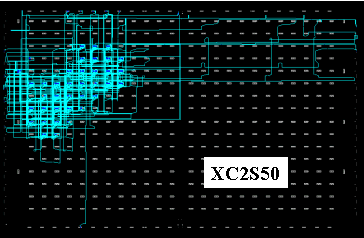
By exploiting the Xilinx device architecture, it has been possible to create processors such as the KCPSM, which occupies just 35 CLBs in a Spartan-II™. The plot below shows a single KCPSM in an XC2S50 Spartan-II device. You can actually fit 8 PSM processors in this device and still have 30% of the device remaining for hardware circuits. Even the smallest Spartan-II (2S40) can support 2 of these PSMs.
I know that many of you have enjoyed using this macro and I never cease to be amazed at the applications you find for it. For many applications, a single PSM combined with hardware circuits has been more than adequate. For applications requiring more processing power, the ability to use multiple KCPSMs in a single Xilinx device has the added advantage of distributing the processing and keeping the interfaces-to-hardware circuits simple and independent. The introduction of MicroBlaze and PowerPC cores has only increased the usage of PSM macros. These tiny processors can handle tasks independently to the main processor and with much tighter and predictable coupling to the hardware circuits.
In this techXclusive mini-series, I will explain how I derived the architecture of KCPSM and how it exploits the architecture of the Xilinx FPGA devices. I hope you will be inspired to create your own application-specific PSM processors as well as find new applications for existing PSM macros.
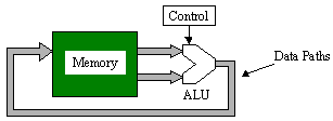
How many bits should a processor have? The nice thing about an FPGA is that you can decide what is most suitable for your applications and implement the data width that you require. In general, the wider the data width, the more logic you will need to support it, and the more capable the processor will become. Conversely, the narrower the data width, the smaller the implementation, but the lower the arithmetic performance. My primary objective was a small size and low cost, so this meant a narrow data width and acceptance of the accompanying lower arithmetic performance. As the processor is surrounded by programmable hardware that offers the ultimate in high performance, the processor was intended to be a complex programmable state machine and not a DSP processor.
Even so, I found it very hard to decide on a bit width, as I did not have one specific application in mind. So when I designed my first PSM in 1993 using XBLOX™ (Anyone remember that one? It was fundamentally a schematic synthesis tool), I avoided the issue by creating a processor in which the data width was defined only at the point of synthesis. It turned out to be quite difficult to construct a processor around this decision, and this lead to many other restrictions, especially when combined with the limits of the XC4000™ devices then available. However, it proved to me that efficient PSM processors could be made, and I started to gather feedback from the most important people -- our customers. Of the people that used this first PSM, nearly all defined an 8-bit data width. It was a simple case of conformance!
Given the choice of conforming to a standard of 8, 16, or 32 bits, the future PSM processors just had to be 8 bits. Not exactly a sound engineering decision, but I learnt never to fight with nature! However, I would ask you to consider "non-standard" bus widths if it fits with your needs.
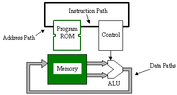
A PSM, like any other processor, will execute a program. A program is formed by a set of instructions that are defined by the user and held in a memory. Each instruction is encoded into a machine code. That much is obvious, but where should that program be stored?
If you use a standard processor, it may be natural to think of the program being stored in a ROM or RAM device, or even on a floppy disk. But if you were implementing a state machine as part of your Xilinx FPGA design, you would not connect any external components. It was clear to me that a PSM must be 100% embedded in the device and totally self-sufficient. In this way, you can make the decision to use one or more PSMs anywhere it makes sense to do so without concern for the design of the PCB on which the FPGA is sitting. This meant that the program had to be implemented inside the device.
Unfortunately the XC4000 family did not contain any dedicated memory, so the CLBs had to be converted to program ROM. However efficient the processor, this ROM was expensive, so programs had to be small and very efficient. Imagine my joy at seeing block RAM appear in Virtex™! Here were 4096 bits of memory just asking to hold a PSM program.
In Peter Alfke's techXclusive "Using Leftover Multipliers and Block RAM in Your Design", we can see that a block RAM can be used to implement a state machine. This is similar in many ways to the way a PSM works, but it does not exploit the dimension of time. The result is a relatively simple state machine that operates very quickly. With a PSM, we can achieve very complex state machines that work relatively slowly.
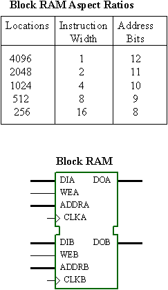
Block RAMs are very flexible in aspect ratio and are initialisable. It would again be very awkward to have to go through a program memory-booting phase before the state machine could become active. However, since all 4096 bits of each block RAM are defined in the configuration bit stream of the device, the PSM is able to operate from the very first clock edge.
So, the block RAM of Virtex (which then became the basis of Spartan-II devices) was to be the program ROM. This defined the second major limit for the PSM in that the size of program would be limited to that supported by one block RAM.
Embedding the program ROM inside the FPGA has the advantage that all of the inputs and outputs of both the program ROM and the processor are "virtual pins" within the FPGA fabric. This means that there is no need to consider bus sharing to reduce the number of pins and busses. It is also obvious that a Harvard architecture is the natural selection. All the requirements for multiplexed data and instructions that would waste time, rather than exploit it, are avoided.
Given that there is no real restriction on the number of virtual pins the PSM can have, it is possible to explore all of the aspect ratios supported by the block RAM. At first, it may appear reasonable to adopt 8-bit instructions to be the same as the data path. This would make sense in a shared memory and bus system, but here we do not need to be constrained in that way.
By having a narrow instruction width, we have the advantage of more program memory locations, but a greater need to encode instructions. It will also be necessary to have fetch cycles to obtain operands when required. This will increase the amount of decoding and sequencing logic and lower performance due to the number of cycles per instruction. As multiple locations will be needed for many instructions, having more memory locations does not actually imply that the program can be longer.
Opting for a wider instruction path means that less decoding logic is required, and there is the potential for each instruction to be completely self-contained in terms of operation and operands obviating the need for fetch cycles. Given the desire to keep the PSM small, it was therefore decided that the 256×16 aspect would be most suitable. Admittedly, a program of only 256 instructions was going to be a constraint, but the intention was to implement a complex programmable state machine rather than full-blown data processor.
In the next article I will consider the relative merits of register, stack, and accumulator processor architectures when a PSM is implemented in a Xilinx device.
If you want to have a look at the KCPSM, it is available for download at the address below. (There is also full documentation and an assembler for you to use.)
Xilinx Application Note 213: "8-bit Microcontroller for Virtex Devices"
This is suitable for all Virtex, Virtex-E and Spartan-II devices. If you would like a PSM specially tuned to the Virtex-II architecture, drop me an e-mail at ken.chapman@xilinx.com and I will be pleased to send it to you.
![]()
|
|
|
|