![]() Technical Information: PicoBlaze Soft Processor
Technical Information: PicoBlaze Soft Processor
|
|
|
|
Creating Embedded Microcontrollers (Programmable State Machines) - Part 2 |
| Back to Creating Embedded Microcontrollers (Programmable State Machines) |
| Author: Ken Chapman | Publication Date: 03/28/2002 |
In the first part of this series, I examined the concept of a programmable state machine (PSM). The idea of this is to offer the ability to define a software-programmable complex state machine and exploit the "time domain" available to achieve a function in a small, cost-effective form. From this concept, and with some consideration for block RAM, we know that the PSM being studied will have an 8-bit data path, along with completely separate address and instruction paths to a program that is stored in a 256×16 aspect program ROM.
Before starting on the details of implementation, we are required to choose a processing architecture.
There are three fundamental architectures in which the data memory and Arithmetic Logic Unit (ALU) can be organised. Hybrids of these also exist, but we will focus on the basic forms to make a selection that is most suitable for a PSM.
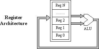
The register architecture has a finite number of registers that the program may select in any order. This tends to make manual programming (i.e., writing at assembler level) a straightforward task. It is desirable to have a large number of registers to perform complex tasks and hold multiple variables locally. Obviously, the more registers there are, the larger the implementation of a processor due to the number of storage elements and the multiplexer logic that is required to select the operands applied to the ALU.
Equally significant is the impact a register-based architecture has on instruction size. Some bits must be used to specify each register used in an instruction. For example, a 3-bit binary code is required to select one of 8 registers. Therefore, 6-bits would be required to specify the two operand registers. A further 3-bits may be required to specify a destination register for the result.
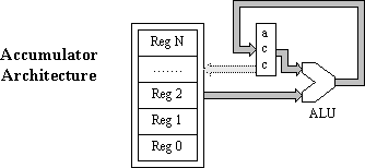
The accumulator structure is almost certainly associated with registers or memory to hold the various variables. The advantage of the accumulator structure is that one of the operands and the destination for the result is implied and does not need to be specified in the instruction encoding. Hence, the instruction encoding only needs to reserve bits to identify the remaining operand, and less logic is required to select the register or alternative source.
The disadvantage of this structure is that a program will tend to expend instructions and time simply moving an initial value into the accumulator or storing the accumulated value. Whilst long sequences involving the current accumulated value will be efficient, more esoteric programs, such as those implementing complex state machines, will become tedious to write and be slow to execute as the accumulator is continuously initialised and stored.
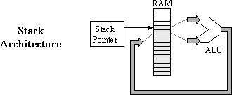
The stack architecture is probably the most efficient in terms of silicon resources, as it links directly to memory that is forming the stack and requires no data selection logic other than the stack pointer. The instruction encoding is also very efficient because the location of both operands and the result are implied as being the top of the stack.
However, even more instructions (stack PUSH and stack POP) are expended to ensure that the correct data is located at the top of the stack. Correct sequencing of the ALU operations will result in excellent code density and execution speed, but this "reverse polish" style does not come naturally to most of us and greatly impacts the desire to utilize a PSM that provides an easy methodology for implementing complex state machines.
{- The stack architecture is not the best choice, as the methodology is
too cumbersome.
- The accumulator structure seems reasonable, but
expending too many instructions to move data is a concern given limited
program memory space.
- The register architecture appears to be the
best for PSM applications, but it could be expensive.
The cost of implementing a register bank can be high, as the following diagram illustrates. Only four registers are being implemented; there are 32 flip-flops for 8-bit data, which would occupy 16 "slices" of a Spartan-II™ or Virtex™ device.
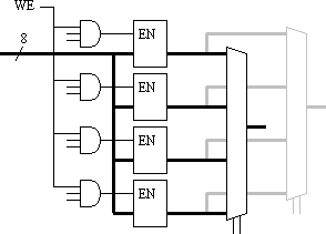
We must now add the operand selecting multiplexers and clock-enable gates to the registers. A 4-to-1 multiplexer would require a complete slice per bit by combining the two LUTs and the dedicated MUXF5. Hence the 8-bit multiplexer requires 8 slices.
To fetch both operands at the same time, a second multiplexer is required. This 16-slices of logic is free if the combinatorial logic is mapped into the same slices as the flip-flops. However, placing combinatorial logic between the registers and the ALU would compromise the performance of the processor. The clock-enable gates only require 2 slices, but again would add combinatorial delay.
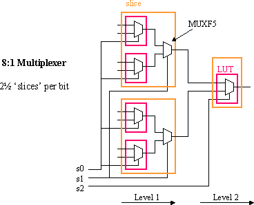
Increasing the number of registers does not seem to be a good idea! The table below illustrates the number of slices required by a Spartan-II to implement a selection of register bank sizes. Whilst it is obvious that more flip-flops are required, the multiplexer logic dominates the size. The multiplexers for 8 and 16 registers also incur another level of logic delay as indicated by the 8:1 multiplexer above. Virtex-II has dedicated MUXF6 and MUXF7 components that help reduce the size of larger multiplexers and significantly increase performance.
So, it appears that the desire for more registers that will make a PSM easy to use must be balanced with the expense of implementation in both size and performance. Fortunately, this is where one of the most powerful features of Xilinx devices comes into play...
The SRAM configuration cells normally used to set the "gate" functionality implemented by a LUT are also available within the design directly as RAM. Hence each LUT offers 16 bits of RAM, and a "slice" can provide 32 bits of RAM. Of particular interest to PSM development is the ability to trade 16 bits of RAM per slice in order to achieve a type of dual-port RAM that is ideally suited for implementing a register bank.
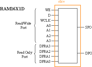
The 16 RAM cells provide all the functionality of a 1-bit, 16-register bank, complete with selective write enable. The second port enables a second operand to be accessed in the same way that a second multiplexer was used with discrete registers. With this great feature, an 8-bit, 16-register bank can be implemented in just 8 "slices" (compared to 88 "slices") and significantly increases performance.
Given the potential offered by these 8 "slices", it is easy to see why a register-based architecture should be considered and why it makes sense to include 16 general-purpose registers in the Virtex-E and Spartan-II PSM implementation.
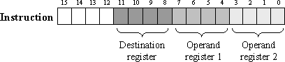
In Part 1, I described how the 256×16 aspect ratio appeared to be advantageous for storing the program. Now that we have selected a register-based architecture and seen the potential for 16 registers, we can consider the initial format of the instruction encoding.
It is also necessary to consider operations involving a constant value. It is desirable to keep all instructions self-contained, so an 8-bit constant must be specified within the instruction encoding together with the register operands.
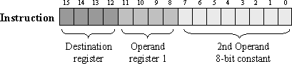
Clearly, the instruction now has to specify so much operand information that there is simply no space to define the operation. Although exploiting both ports of the block memory could form a wider instruction format, the even wider aspect ratio would further reduce the program length (128×[16+16] aspect ratio). Alternatively, we could consider using a fetch cycle to obtain constant values, but this again would reduce program length and lead to variable instruction size and duration.
Given the desire to keep all instructions self-contained and maintain the natural 256×16 program ROM aspect ratio, a compromise must be made. In this case, the destination register was inferred by making it the same as the first operand register. This releases 4 valuable bits of instruction for encoding the operation and reveals the primary encoding for all ALU-related instructions.
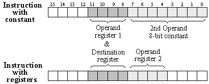
It is clear that the programming may not be quite so flexible, and that additional instructions will be required when the first operand register contents must be preserved. However, program coding can often be organised such that this is not such a restriction, and can even be advantageous in the same way as an accumulator. The ability to specify a constant as the second operand (at no cost to program size or performance) will also be valuable when defining the instruction set. (I will study this later in the series.)
The structure of a PSM is already emerging. Through this very simple and progressive analysis, we can see how important memory is to a processor and why the Virtex and Spartan-II devices are well-suited to this application.
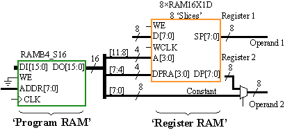
The program memory acts as the controller and is formed using block RAM. The variable data will be held in registers, and these are made cost-effective via the highly efficient distributed dual-port RAM. Without this distributed RAM option, the 44 CLBs (88 "slices") required to implement the register bank alone would already exceed the size of the complete PSM implementation!
In the next article, I will define the program flow control instructions, then examine the details of implementing the program address counter and associated logic. Here, we will see a third way memory can be used in our time-sharing machine.
If you would like to have a look at KCPSM, you may download it at the address below. Full documentation and an assembler are also available.
XAPP213 "8-bit Microcontroller for Virtex Devices":
http://www.xilinx.com/xapp/xapp213.pdf
ftp://ftp.xilinx.com/pub/applications/xapp/xapp213.zip
This is suitable for all Virtex, Virtex-E and Spartan-II devices. If you would like a PSM that is specially tuned for the Virtex-II architecture, drop me an e-mail at ken.chapman@xilinx.com, and I will be pleased to send it to you.
![]()
|
|
|
|