![]() Technical Information: PicoBlaze Soft Processor
Technical Information: PicoBlaze Soft Processor
|
|
|
|
Creating Embedded Microcontrollers (Programmable State Machines) - Part 3 |
| Back to Creating Embedded Microcontrollers (Programmable State Machines) |
| Author: Ken Chapman | Publication Date: 03/28/2002 |
In Part 2, we decided that the program will be stored in a 256×16 aspect block RAM and that the fundamental processing architecture will be 16 registers implemented with the highly efficient distributed dual-port RAM. We will now consider the detail of the implementation.
Part 3 will focus on program flow control aspects and define the instructions required to control a program execution sequence. We will then consider the implementation of the program counter and its associated circuits and realise again that RAM is highly desirable in this "state machine" section of a PSM.
A traditional processor executes instructions one at a time from sequential memory locations of the program memory. Execution normally starts at memory location zero. This the reason for the requirement of a program counter (PC), which increments through the program memory locations.
The simple "increment" operation of a program counter is very efficient and easy to implement in the Xilinx Virtex™ and Spartan™-II devices. Dedicated carry logic components and flip-flops within each logic "slice" are all that is required to implement a simple incrementing counter.
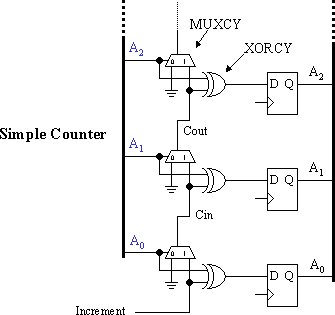
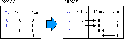
The carry logic is able to implement an increment function without using the look up table (LUT). The operation of each bit is defined by the following truth tables. Observe how the MUXCY propagates the carry signal.
Because each logic "slice" contains the carry logic components and flip-flops for 2-bits, the required 8-bit program counter to access 256 memory locations can be implemented in just four "slices". However, the program counter must do more than increment.
As a minimum, the PSM processor should have a way to repeat sections of code by enforcing the program counter to non-sequential address locations. The ability to jump (or branch) to any specified program memory location would allow for greater programming flexibility. To make a processor practical, the jump would be performed only under specified conditions (conditional jump) so that different sections of code are executed under different circumstances.
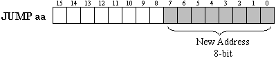
In Part 1, we decided that the 16-bit aspect ratio of the block RAM was more suitable for a PSM as it would enable the operands to be included within each instruction. With a JUMP instruction, the operand is the desired program counter value after execution; therefore, the JUMP instruction must specify an 8-bit address for the PSM program counter.
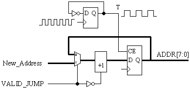
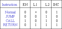
Now, the program counter must be loadable. When the instruction coding indicates that a JUMP must occur, the normal counter feedback must be replaced with the new value and the increment prevented. The LUT associated with each bit of the counter is now ideal for implementing the multiplexer to perform this selection.
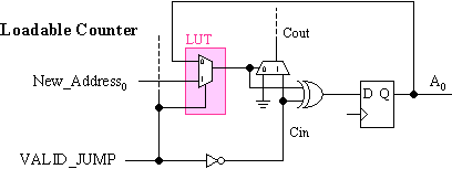
The VALID_JUMP signal will be active-High when a JUMP instruction is detected and when any conditions that are imposed on the execution are met. This will be a logical decode based on the remaining 8 bits of the instruction word and flags from the ALU. The inversion of the VALID_JUMP signal is used to drive the input to the carry chain to prevent the new address value from being incremented as it is loaded. This inverter is absorbed into the dedicated carry logic such that it requires no additional resources and does not impact performance.
The JUMP instruction indicates that a decision will take place, and control over this decision implies the need for timing on the PSM. On the next clock edge, the program counter will either increment or load. The JUMP instruction therefore requires one clock cycle to determine which address of program memory will be accessed next.
The program is stored in block RAM. It now becomes crucial to realise that the block RAM is a synchronous memory which must be clocked to both write and read data at a given address. Hence, if the program counter takes one clock cycle to determine the address, and the block RAM takes another clock cycle to access the instruction located at that address, the fundamental operation of a PSM takes two clock cycles per instruction.
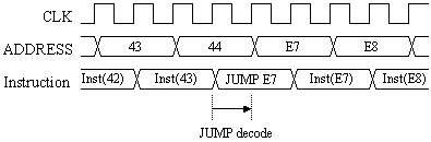
In the above timing diagram you can see that most instructions result in the simple increment operation of the program counter. When the JUMP instruction located at address 44 is read from the block ROM, the program counter is loaded with the new address value supplied (E7) and the address jumps on the next clock edge.
The decoding of a JUMP instruction must take place in one clock cycle. All other instructions can be completed in two clock cycles; we will exploit this in the ALU and I/O instructions later. Although it is possible to execute all non-JUMP instructions at one-clock intervals, the handling of a JUMP instruction becomes more complex and detracts from the concept of the PSM being small and simple. The constant two clock cycles for every instruction also makes execution time easy to predict when writing a program. Processor terminology refers to the two cycles per instruction as T-states.
To make the program counter change only every two clock cycles, the dedicated clock enable on each of the counter flip-flops can be controlled using a simple toggle flip-flop.
The toggle flip-flop is essentially the only logic forming the "state machine" of the PSM. The counter logic exploits the capability of the four "slices" very well.
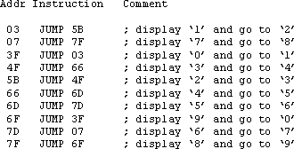
With only a JUMP instruction, we can already see that a program can be written for the programmable state machine. In this simple example, the address signals are used to drive a 7-segment display directly. The program is written to ensure that the address sequence provides a decimal counter on the display. The display would change every two clock cycles.
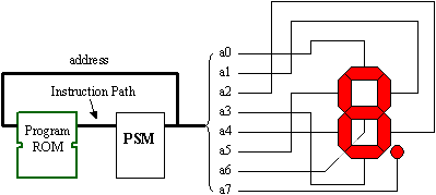
Whilst this simple example may be an interesting concept, it is unlikely to be a practical way to work with a PSM. However, the advantage of a fully embedded processor is that all signals are available to interface with the programmable logic of an FPGA. By organising programs to have routines located at particular addresses, it is possible to decode these addresses and trigger events external to the processor (but still internal to the FPGA) without actually performing I/O operations.
The PSM is intended to be a practical way to exploit time and share logic. A subroutine extends this concept by enabling sections of common code stored in memory to be shared by different parts of the program. Code does not need to be "in line," and this makes it potentially more compact and easier to write. Given the restricted program space of a PSM, a feature that enables compact code is highly desirable. Anything that makes writing a program easier is always desirable!
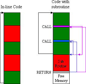
The CALL instruction is similar to a JUMP instruction in that the operand will again provide a new address to be loaded into the program counter provided conditions have been met. The RETURN instruction also causes the program counter to load a new address at the end of the subroutine. However, unlike the JUMP or CALL instructions, there is no operand to specify the new address; this must be derived by the PSM itself. To achieve this address specification, the CALL instruction must also store the current program counter value.
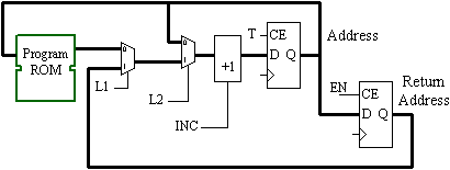
A register connected to the program counter is able to capture the address value when a CALL instruction is encountered. When the RETURN instruction is detected (at the end of the subroutine), the value from this register can be loaded back into the program counter. The program counter now has two sources of new address information, and a second multiplexer is required to make this selection, requiring four additional "slices". Closer inspection reveals that during a RETURN instruction, the return address value must be incremented as it is being loaded so that the instruction following the original CALL is executed.
Careful allocation of instruction op-codes means that the decoding logic to control these signals can be very simple, and that sometimes an instruction bit can drive a control directly.
The register used to preserve the address value is formed of eight flip-flops and therefore occupies another four "slices". In Part 2 we saw how distributed dual-port RAM could very efficiently provide a register bank, and now we can exploit distributed RAM in single-port mode to provide an address stack.
With a program address stack, nested subroutines can be executed, making programs even smaller and easier to write. Because the program address stack is implemented independently of the ALU, registers, and I/O, no special instructions or programming styles are required to initialise or control the stack operation.
To form a stack, a 4-bit up/down counter requiring two "slices" is used to address the distributed RAM. When a CALL instruction is encountered, the current program address is pushed onto the stack by writing the memory and incrementing the stack counter. RETURN instructions will decrement the stack counter and read the program address from the distributed RAM.
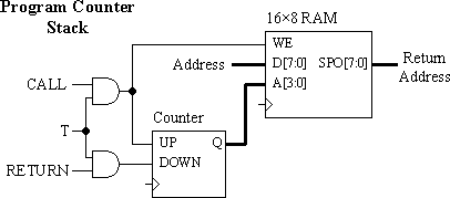
Due to the two cycle per instruction format, the CALL and RETURN instruction decoding must be qualified by the T-state control such that the stack is only "pushed" or "popped" once. Although there are two clock cycles per instruction, only one cycle is available to decode a JUMP, CALL, or RETURN instruction and load the program counter. The operation of the stack should therefore be arranged such that the "top of stack" return address is presented at the output of the stack at the start of each instruction execution in case it is a RETURN operation.
We can now see that the PSM employs RAM three times, each with independent address and data paths. Although the simple instruction decoding logic is not shown, the fundamental program flow control has been achieved using just 14½ "slices".
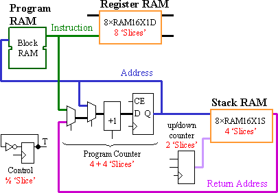
Distributed RAM has been used twice to provide a total of 256 bits of memory in 12 "slices". Using flip-flops and logic to replace these memory structures would require 152 "slices", which is more than double the size of the complete KCPSM (35 CLBs in Spartan-II provide 70 "slices"). Using block RAM to implement these small memories would be wasteful and would impact the flexibility of a PSM to be used multiple times in devices, especially small ones with limited block RAM.
In Part 4, we will define an instruction set for the PSM and discover that efficient multiplexers are the key to the implementation of the ALU.
To have a look at KCPSM, download it from the address below. Full documentation and an assembler are also available. More than 1000 copies of KCPSM are downloaded from the web site every month. If you already use KCPSM in your designs, it would be great to hear from you, and I look forward to your emails.
XAPP213 "8-bit Microcontroller for Virtex Devices"
http://www.xilinx.com/xapp/xapp213.pdf
ftp://ftp.xilinx.com/pub/applications/xapp/xapp213.zip
This PSM is suitable for all Virtex, Virtex-E, and Spartan-II devices. If you would like a PSM specially tuned to the Virtex-II architecture, drop me an e-mail at ken.chapman@xilinx.com and I will be pleased to send it to you.
NOTE: Xilinx has recently given the KCPSM reference design the name "PicoBlaze," to indicate the complementary nature of the Programmable State Machines with the high performance 32-bit RISC soft processor called "MicroBlaze" that was released in October 2001. With PicoBlaze(TM) and MicroBlaze(TM), designers now can choose from a range of "right-sized" solutions, from 8 to 32 bits.
![]()
|
|
|
|