![]() Technical Information: PicoBlaze Soft Processor
Technical Information: PicoBlaze Soft Processor
|
|
|
|
Creating Embedded Microcontrollers (Programmable State Machines) - Part 4 |
| Back to Creating Embedded Microcontrollers (Programmable State Machines) |
| Author: Ken Chapman | Publication Date: 03/28/2002 |
At last, we may define the ALU instruction set of our PSM. Whilst the ALU would appear to be the logical starting point for any processor design, I hope you have been able to see that it is better to design a PSM starting first with the considerations of the "life support system" surrounding the ALU. In this way, we have derived the format of the instruction words (16-bit), the number of registers (16), and the necessity to infer the destination register for operations requiring two input operands.
Another reason for leaving the definition of the ALU instructions until the end of your design process is because this is an area of great deliberation and debate. Can you imagine the long discussions and arguments occuring at companies that design and manufacture microprocessor chips? There must be enough instructions so that the chips are easy to use, but every instruction added makes the processor more expensive to manufacture. Sometimes special instructions may be included to make the processor more suitable for certain applications (such as a hardware multiplier for improved DSP performance), but such specific tuning may then preclude that processor from being adopted for other applications. Of course, any special instructions are only valuable if they are actually used, which may not always be the case if the compiler or software engineer does not invoke them when the opportunity arises.
The advantage of creating a processor inside an FPGA is that the ALU instruction set does not have to be fixed until you decide it is right for you. You may actually define a different instruction set to suit each particular application. In practice, you will probably find that defining one personalised instruction set is adequate unless you implement a very diverse range of products. Even if you discover that you made a poor choice of instruction set well into your design phase, you still have the ability to change it. However, be careful not to make changes too often as this will impact the development time of your product and detract from the advantages the PSM concept offers in the first place.
When I defined the instruction set for my KCPSM (PicoBlaze™) macros, I wanted to provide a reasonably general-purpose machine that could be applied to a wide variety of applications. My focus was also to keep the size small, so I avoided including any logically expensive operations that would be infrequently used. It was always clear to me that whatever I chose could be changed in future, so I did not loose sleep over my decisions! Provided that you have a reasonable selection of basic instructions, it should be possible to write programs (or sub-routines) to perform more complex operations. For example, repeated shift and addition operations may be used used to realise a multiplication.
Electing to include a particular operation in the ALU will probably make the PSM larger. However, it will mean that your programs should become easier to write and will execute more quickly. Generally, the concept behind a PSM is to perform complex state machine tasks that are not particularly time critical; therefore, adding logic to the ALU so that programs will execute faster is not high on my priority list, but obviously your objectives may be different. The more significant advantage of adding a special operation is linked to the phrase that programs become "easier to write". The ability to specify one instruction instead of multiple operations not only makes programming easier, but implies a smaller program. Since the most restrictive aspect of a PSM is the length of the program stored in block RAM (256 locations in Virtex™-E or Spartan™-II, and 1024 locations in Virtex™-II), being able to write more compact code can be vital for a successful fit.
A program that nearly fills the available block RAM and executes at an acceptable rate indicates efficient use of the device via time-sharing of the logic resources. Use this to gauge whether it is necessary to include special instructions to make the code smaller and faster.
The format of the ALU instructions for my PSM macro was partially defined in Part 2. The first operand will be a register (sX), which also implies the destination for any result. The second operand can be register (sY) or an 8-bit constant (kk). There are also instructions that only manipulate the contents of a single register (sX). Part 3 illustrated how JUMP, CALL, and RETURN instructions provide flexible flow control of the program. Although not strictly an ALU operation, we must also consider that the PSM processor will need to communicate externally using some form of input and output ports. My choice for these input/output (I/O) operations was to allow values to be passed to or from a register and a port specified by an 8-bit address. This has the same operands as other ALU operations except that the second operand is used to provide the port address.
Instructions may be formed into groups with common operand types:
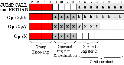
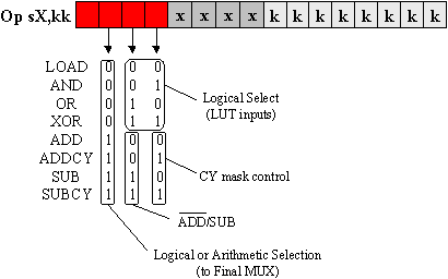
Given that the instruction words are 16-bits, it is clear that only 4 bits are available to uniquely encode the principle instruction groups. Fortunately, this does not mean that only 16 (24) instructions are allowed in total, because most of the groups contain "spare bits" that can be used to encode instructions within the same group. You can see that the "OPsX" group has 8 "spare bits" with the potential for up to 256 (28) instructions within the single operand group. The "OPsX,sY" and JUMP, CALL, and RETURN groups each have 4 "spare bits" with the potential for a further 16 (24) instructions in each group. Therefore, the greatest constraint comes in the "OPsX,kk" group where no "spare bits" exist.
The "OPsX,kk" is the original reason behind the decision to infer the destination register to be the same as the first operand (see Part 2). It is now obvious that this instruction group must be fully encoded by the primary 4 bits, which must also be used to identify the other groups. Therefore, the maximum number of instructions in this group is 13 (or 14 for those who really want to push it!).
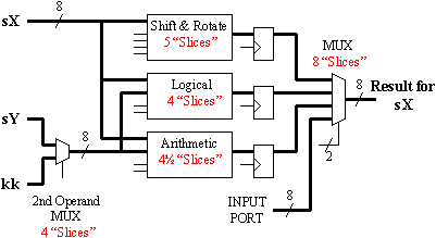
The key to an efficient ALU implementation is reducing the amount of multiplexing logic. In the most primitive implementation of an ALU, every operation is performed in parallel regardless of the instruction being executed at the time. The instruction decoding logic then selects the appropriate result. To make the following descriptions easier to understand, I will focus on my implementation of the KCSPM (PicoBlaze) instruction set. The 18 ALU-based instructions certainly require a great deal of multiplexing. There is also the simple 2:1 multiplexer to choose either a register or constant value for the second operand (introduced at the end of Part 2).
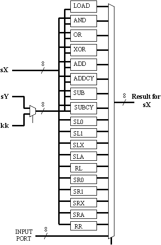
The apparent requirement for a 19-input multiplexer is alarming! Even with the dedicated multiplexers within the logic slices (MUXF5 etc), the size of this multiplexer for the 8-bit data width would be 48 "slices". This is very expensive, considering that each actual ALU function has yet to be implemented. This multiplexer would also require 5 select lines -- it would be an interesting task to encode these from the 4 primary bits and various "spare bits" of the instruction words.
Obviously, the amount of multiplexing may be reduced by decreasing the number of available ALU operations, but this hardly the most desirable solution! In Part 2, we saw that multiplexers could be very expensive in a register-based processor structure, but we avoided this situation by using the look-up tables in a RAM mode. We must now see how the look-up tables may be exploited to combine some multiplexing with the ALU operations that must be implemented.
The logical group of instructions provide bit-wise logic operations between two operands. If the set of operations is drawn out in more detail together with a multiplexer, we make a powerful observation:
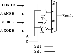
For each bit of the operands, we can see a 4-input function -- a perfect fit for a look-up table. In this way, the entire 8-bit logical group (including the multiplexer) can be realised in just 4 "slices" rather than 20 slices (4 "slices" for each AND, OR, and XOR, plus 8 for a 4:1 multiplexer). This reduction in size again provides the benefit of higher performance.
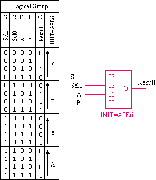
The above truth table derives the INIT value for each LUT forming the logical group. The same mapping should be achievable via synthesis tools now that we are breaking the description of the ALU down into manageable pieces.
The Arithmetic group performs an 8-bit addition or subtraction with or without the inclusion of a CARRY flag. The first reduction can be made simply by reordering the description of the optional CARRY operation:
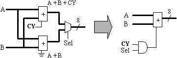
Rather than use the select signal as a multiplexer control, we now use it as a masking control to the CARRY (CY) signal. Since this is a single AND gate, it only costs a ½ "slice" compared with 4 "slices" for a multiplexer and a further 4 "slices" for a second adder. Although this is a simple observation, you must consider this when writing any HDL code.
More knowledge about the arithmetic capability of the Xilinx devices tells us that the addition and subtraction operations may also be combined. This is also a case of reordering the functions in order to place the multiplexer in front of the carry logic. Subtraction is performed in the "slices" -- the addition of the "A" input with the twos complement of the "B" input. To perform the twos complement of "B", each bit of "B" is inverted (the one's complement), and the addition of "1" is achieved by applying a carry input to the adder.
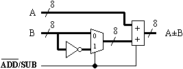
Making the complement of the "B" optional requires a multiplexer, but there is no problem absorbing this into the function generator, which performs the "half add" preceding the dedicated carry logic. This rather complex-looking function generator reduces to a 3-input function and is more typically represented as a 3-input XOR gate.
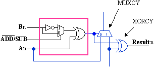
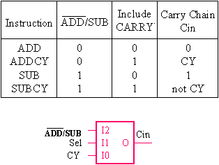
The input to the carry chain must combine the effects of the twos complement addition of "1" with the optional addition of the CARRY flag. This reduces to a 3-input function and therefore occupies no more space that the simple masking AND gate required for the optional carry input adder. The most complicated cases of this table involve subtracting. The simple SUB operation means that the input to the carry chain must be forced High to provide the twos complement addition of "1". When performing a SUBCY operation, the CY input must be inverted such that when CY=0, the twos complement addition of "1" still takes place. When performing a SUBCY operation with CY=1, the the inverted CY prevents the twos complement addition of "1" so that the result is the required A-B less one (i.e., A-B-CY where CY=1).
Now, the entire arithmetic group is implemented by just 4 ½ "slices" rather than 24 "slices" (4 "slices" for each add or subtract, plus 8 for a 4:1 multiplexer).
The shift and rotate group is a simple case of selecting the correct bits via multiplexers; it is obviously reduced to the following structure:
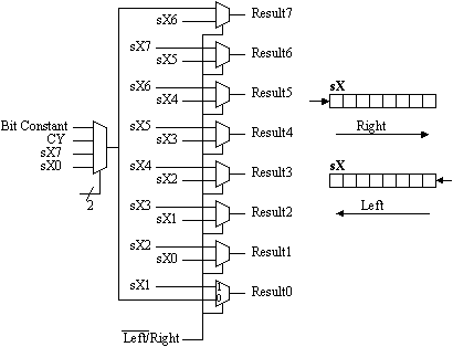
Anyone familiar with KCPSM (PicoBlaze) may have wondered why the shift and rotate group is so comprehensive. When examining the above structure, we can see that all the operations share the same 2:1 multiplexer created in 4 "slices". A single "slice" is then required to select the information to be injected into the MSB or LSB of the result. The multiplexer select lines and the "Bit Constant" are easily provided using 4 of the 8 "spare bits" available in the "OPsX" group.
Some final multiplexing is required to combine the three main ALU instruction groups and provide an input data port. This final 4:1 multiplexer is efficiently implemented by 8 "slices", including the MUXF5 dedicated multiplexers. If you create your own ALU, this final multiplexer is always worth careful consideration. The 4:1 is a perfect fit in the Xilinx architecture. There is nothing to be gained from having a 3:1 multiplexer, but a 5:1 would be larger and add delay with associated lower performance. The next natural fit would be an 8:1 multiplexer at a cost of 16 "slices".
In Part 3, we saw that the PSM would work with a constant 2-clock cycles per instruction. This means that the ALU has 2 clock cycles in which to complete any operation. The path through the ALU would certainly become the critical delay path and set the performance of the the PSM as a whole. Although time specifications could be applied to indicate these 2-cycle paths, there are plenty of flip-flops available to insert a pipeline stage and simplify all time specifications to the normal clock period.
The size of an ALU will depend on the instruction set that you define. However, I hope you can apply similar techniques that I have used to implement the KCPSM (PicoBlaze) ALU in 25½ "slices". Remember to see which functions can be reordered and combined to minimise the actual number of logic blocks working in parallel and reduce the size of the final multiplexer.
All the reduction also helps to simplify the task of decoding the instruction words and controlling the select lines on each of the ALU blocks. Indeed, if you are allocate the instruction encoding carefully, many of the bits can be applied directly to the ALU blocks, as illustrated by the most constraining "OPsX,kk" operations of KCPSM (PicoBlaze).
The ALU also generates flags used in some operations (i.e., ADDCY) and program flow control. KCPSM has a CARRY flag and a ZERO flag, but you may decide that other flags are more useful in your own PSM processors. Each flag may be implemented using a simple clock enable flip-flop to ensure that they are only updated during appropriate ALU operations.
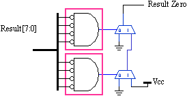
The CARRY flag is forced to zero during logical operations and captures either the carry chain output during arithmetic operations, or the bit "shifted out" during shift and rotate operations. The CY flag is therefore driven by a simple 1-bit multiplexer.
The ZERO flag is set when all bits of the result from any operation are low. This is a simple 8-bit NOR operation and can be efficiently implemented within a single "slice". As well as saving a LUT, the use of the carry chain in this way ensures a minimum delay. Delay in forming the ZERO flag value can be critical, as it follows the final MUX of the ALU.
In the final article of this series, I will present some alternative architectures to consider when implementing a PSM, make some comments about programming tools, and discuss a few possible applications of a PSM. It would be great to include some of your applications as examples, so do keep letting me know what you are using KCPSM (PicoBlaze) for yourself.
To have a look at KCPSM, download it from the address below. Full documentation and an assembler are also available. More than 1000 copies of KCPSM are downloaded from the web site every month. If you already use KCPSM in your designs, it would be great to hear from you, and I look forward to your emails.
XAPP213 "8-bit Microcontroller for Virtex Devices"
http://www.xilinx.com/xapp/xapp213.pdf
ftp://ftp.xilinx.com/pub/applications/xapp/xapp213.zip
This PSM is suitable for all Virtex, Virtex-E, and Spartan-II devices. If you would like a PSM specially tuned to the Virtex-II architecture, drop me an e-mail at ken.chapman@xilinx.com and I will be pleased to send it to you.
NOTE: Xilinx has recently given the KCPSM reference design the name "PicoBlaze," to indicate the complementary nature of the Programmable State Machines with the high performance 32-bit RISC soft processor called "MicroBlaze" that was released in October 2001. With PicoBlaze and MicroBlaze™, designers now can choose from a range of "right-sized" solutions, from 8 to 32 bits.
![]()
|
|
|
|