![]() Technical Information: PicoBlaze Soft Processor
Technical Information: PicoBlaze Soft Processor
|
|
|
|
Creating Embedded Microcontrollers (Programmable State Machines) - Part 5 |
| Back to Creating Embedded Microcontrollers (Programmable State Machines) |
| Author: Ken Chapman | Publication Date: 03/28/2002 |
In the final article of this series, I will examine some alternative techniques to consider when implementing a PSM, make some comments about supporting programming tools, and mention just a few PSM applications.
In my PSM macros, I chose to utilise a single block RAM to store the program. This obviously restricts the size of the program to 256 instructions in Virtex™-E and Spartan™-II devices when we use the 16-bit aspect ratio, which enables the operands to be included with each instruction. Many of you have told me how you have reached this memory limit; therefore, it seems likely that you will elect to have a larger program space if you implement your own PSMs. I will therefore focus on techniques suitable for supporting these larger programs.
Before we take the "easy" option, let us consider ways to work with the PSM structure we have studied so far in this series. It is not unusual to hear from PicoBlaze™ (KCPSM) users who have included two or three processors in a single design. They realise that distributed processing is the solution, which means that each PSM processor then has its own program memory. Although this may sound extravagant at first, this approach reduces the amount of I/O interface logic and has the advantage of totally independent code, which is easier to develop and test. The following diagram illustrates the interface logic to work with just two simple inputs and outputs:
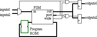
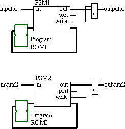
The diagram below shows how the use of two PSM macros simplifies the I/O interface. It may also help with the layout of a design in a large device. (After all, if you were implementing hardware state machines, they would be implemented separately.)
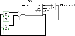
Others have also reported success through implementing a form of memory-swapping under software control. Typically, a sub-routine located at the same position in each program ROM controls the selection by writing to an output port. In practice, it is highly likely that other sections of code will need to be repeated in each of the memory blocks. Hence if two blocks are used, this will not actually yield twice the available program space. This technique does allow a common PSM macro and support tools to be used in a wide range of applications requiring small or "large" programs.
The multiplexer in the above diagram could be saved by using the block RAMs in 512×8 aspect ratio, then using the select bit to address the MSB (9th) address bit. However, the instructions will then be split across the RAM blocks, and programming the ROMs will become more challenging!
Although block-swapping is possible, it does distract from the ease of use that a PSM should offer to a designer. So if a larger program memory really is going to make things easier, we should just consider the impact and use the best techniques.
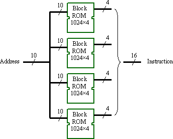
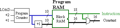
Larger program memory may be constructed by combining several block RAMs. Using CORE Generator™ is probably the easiest way to construct such a memory, given the need to initialise the contents of the memory with the program. Each instruction code will be split across the blocks rather than using the memory in "block pages". Larger memories constructed in this way require no additional logic, as the multiplexing and address decoding is achieved directly by the block RAMs. In the diagram below, a memory of 1024 locations of 16-bits is implemented. Consider the impact of using the same block RAMs organised in 256×16.
Increasing the size of the program memory sounds like an easy thing to do, but the PSM is now required to support the extended address range. To increase from 256 locations to 1204 requires that the program counter grow from 8 to 10 bits. Likewise, the width of the CALL/RETURN stack must grow. However, these only increase the size of the PSM by a few "slices". The real issue is determining how to specify the address operand in the JUMP and CALL instructions.
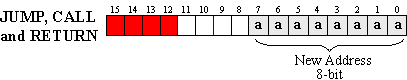
In Part 4, we examined the pressure that existed on the four "primary" bits of the 16-bit instruction word. For this reason, the "spare" bits associated with the flow control group will be used to further encode these instructions. Not only must we distinguish between JUMP, CALL, and RETURN, but we also must encode if the instruction is conditional. This was a pretty tight fit in my own KCSPM design, which allows unconditional and conditional instructions with conditional tests for zero, not zero, carry, and not carry. This leads to a total of 15 combinations, which obviously puts pressure on the 4 "spare" bits.
Now, consider what happens when the address operand grows to 10-bits...
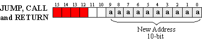
It is clear that there would be no way to encode all the desired instructions in the two "spare" bits that remain. Retaining a 16-bit instruction format would either require a reduction in the number of conditional flow control instructions or place more pressure on the primary bits, causing a potential reduction in ALU instructions. Neither of these is desirable; we should also remember that the more encoded the instructions become, the larger and slower the PSM decoding logic will become.
Traditional processors solve this same issue using a variety of methods:
Operand Fetch: Rather than keep each instruction fully self-contained, operands are obtained from the program memory as required by using subsequent memory locations. This uses up some of the additional memory space we are trying to provide and leads to fetch cycles that complicate the PSM internal state machine.
Relative JUMP: This limits the distance you can "jump" to an address relative to the current location. An 8-bit address operand is typically a twos complement value that allows the program counter to be increased by up to 127 and decreased by up to 128. This works well with small routines, but doesn't make movement between routines very nice. Calls to subroutines outside the range would be impractical. Programming of this type of processor really requires an assembler supporting labels, and the program counter logic must implement a signed addition.
Pre-Fetch Instruction: An instruction is used simply to provide operand information that is then available for use by a subsequent instruction. The operand is loaded into a holding register inside the processor. Once again, this requires a memory location and additional logic inside the processor.
These methods are ideal when the operands can be large in comparison to the available program memory width. They were the only sensible methods to use for full 8-bit data and 16-bit address range processors using external byte wide memory. However, a PSM is intended to be 100% embedded, and it is good to further exploit the flexibility of the devices and the "virtual pins" that the embedded state offers. Since we are only trying to make the address operand a few bits longer, a solution would be to make the program memory wider. At 18-bits wide, the additional 2-bits are provided, and the number of bits available to encode the instruction is restored.
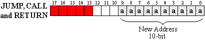
This is not an obvious solution unless you are familiar with Xilinx FPGAs, and it still may not be obvious now. People tend to think in terms of 8, 16 and 32 bits when it comes to processors and memory, so a memory width of 17, 18, 19, or 20 bits sounds strange. In Part 1, we opted to make all instructions 16-bits wide, as that was the widest aspect ratio of the Virtex-E and Spartan-II block RAM. To increase the width by a few more bits does not seem to be a naturally good fit until you combine this with the fact that a larger program memory is implemented by joining multiple block RAMs together, each configured in a deep but narrow aspect ratio.
Hence, five block RAMs in 1024×4 mode implement a 1024×20 program memory. The additional 4-bits now available to describe each instruction will also help reduce the pressure on the primary encoding and make the PSM smaller, faster, and easier to design. Alternatively, they may be used to provide the PSM with more features and instructions.
Virtex-II
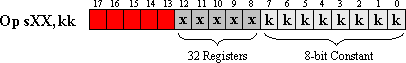
Rather fortuitously for PSM macros, the block RAMs provided in Virtex-II devices are four times bigger than those in Virtex-E and Spartan-II devices, and generally provide adequate memory for PSM-based applications. But the good fortune doesn't stop there. In addition to supporting a 1024×16 aspect ratio on the main data port, these blocks provide an additional bit for each byte of data, with the intention of storing parity information. This means that the memory is actually 18-bits wide when 1024 locations are provided.
In my PSM macro that is specific to Virtex-II (KCPSM-II), which supports the 1024 locations of program space, I also used the additional bits to increase the number of internal registers to 32 (requiring 5 bits to identify) and make the instruction encoding easier. The most demanding "OpsXX,kk" instruction then had 5 primary bits remaining for instruction encoding.
Fetch without Fetch!
There will still be occasions when a PSM would benefit from the ability to specify large operands. Personally, I think it would cease to be a "programmable state machine" if the program length exceeded much more than 1024 instructions. However, it may make sense to implement a PSM with more than 8-bit data, and as previously discussed, that would probably mean a leap up to 16-bits. This really makes it impractical to include constant information within an instruction word because the program memory would have to become so wide that the additional bits would not be used in other instruction groups. It appears that we should return to the concept of a fetch cycle to obtain constant values when required, but we can modify this in the FPGA implementation.
CONSTANT POOL - Given the relatively small size of PSM programs, only a limited number of constants will be in use. Even when the data bus supports 16-bit values, further study of typical programs reveals that many constants are small values (such as "0" used for clearing registers and "1" used when a software counter is incremented). A "constant pool" is an additional memory in which constant values required by the program are stored separately from the program. The operand of the instruction is then used as an index address to this memory in order to locate the required constant. Small constants can still be contained directly in the instruction so that the constant pool may be kept small. Distributed memory is ideally suited to this function.
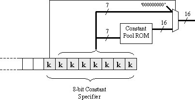
In the above diagram, the MSB of the constant operand is used to specify whether the lower 7 bits should be used directly to supply the constant value in the range 0-to-127, or used as an address to the constant pool to access 16-bit constants in the range 0-to-65535. It is useful to have an assembler to identify the constants that exceed the limit of 127 and build the indexed table of values automatically. Programming requires that both the program memory and the constant pool memory be initialised.
A trade-off occurs when the size of a constant pool is selected. In this example, although 7 bits are available for addressing the constant pool, it is likely that only 4 or 5 bits would be required to address 16 or 32 locations in a distributed memory. If the pool is too small, it is possible that certain programs will require more values than can be stored. If the pool is too large, the PSM will become larger, and there is a point at which the memory would be better used to make the instruction format wider.
PARALLEL ACCESS - This technique is very similar to an operand fetch cycle in that the operand is stored in the program memory location following the instruction. Although this uses program memory space, it has the flexibility to store any number of constants required by the program. As with the constant pool technique, it would still be a good idea to represent small constant values within the single instruction word and reserve the "fetch" for larger values.
The parallel access technique exploits two features of the PSM concept. First, it exploits the dual-port ability of the block RAM to read two locations of program memory simultaneously. Less obviously, but more significantly, it exploits the 100%-embedded nature in order to allow all the additional "virtual pins" that are required to connect the PSM to the program memory for a second time.
The above structure assumes that a 16-bit PSM is being formed in Virtex-II. An additional 26 "virtual pins" allow parallel access to the program memory to access operand information when required. An incrementer is used to access the location following the current instruction at all times. The multiplexer following the memory is used to select between small and large operand values. The program counter must be enhanced to allow it to jump forward by two addresses in the cases when a large operand is stored.
If you design your own PSM, it won't be very long before you are frustrated with manually encoding machine code for it to execute. Besides the time consuming effort of programming in this way, it is also rather prone to errors. As with any complex state machine, a PSM has a potentially large number of "illegal states" that correspond to all the unused instruction word combinations. It is likely that you will need to develop and debug your software program anyway, so having to deal with incorrect machine code is unacceptable. It is therefore important that you also invest some time in providing an assembler to accompany your PSM macro.
Given the restricted size of the program memory, and the anticipation that a PSM works very closely with the hardware that surrounds it, it is my opinion that an assembler is highest level of abstraction that should be considered when programming a PSM. On all occasions that I have been asked if there is a C compiler available for PicoBlaze (KCPSM), a discussion about the application has rapidly revealed that a PSM would not be suitable and that MicroBlaze™ would be a much better choice. Since MicroBlaze is a 32-bit RISC processor it is fully supported with a C-compiler and indeed this would become the most suitable way to write programs for it.
So where do you get an assembler for the PSM you have created? Well I understand that there are some assemblers on the market that can be tuned to a given instruction set, but it may just be fun to write one yourself! Even though my software skills are limited and I am more comfortable writing assembler for a PSM, it only took a couple of days to produce a simple assembler for KCSPM (written in Microsoft QuickBASIC for DOS). If you don't feel like writing one yourself, try asking your software friends. You would be amazed how many of them can produce you something usable in a day and enjoy doing it (although it may cost you a couple of beers!).
I do not intend to explain how an assembler works here, but the principle is relatively straightforward. The majority of my assembler source code is used to identify syntax errors and provide constructive feedback. If you are prepared to be more careful about entering your PSM assembler code, the assembler can focus on the generation of machine code only and will be much easier to write.
TEMPLATE MANIPULATION - Once the assembler has done its job, you are faced with how to get the machine code into the block RAM of the design. Template manipulation is a very easy way to accelerate this process and allows the assembler to output a file that is immediately suitable for use by the Xilinx tools. The assembler reads a template text file of the required format except that the actual data values for the program memory are replaced by a special string of characters. The assembler then identifies these special strings and replaces them with the actual data before writing the modified file out.
The most simple template file for a PSM is a coefficient file for use with the Core Generator. This really only needs to have the "memory_initialisation_vector=" string at the start, but may also include other configuration information used to define the "single-port Block memory" or "dual-port Block memory" cores more completely (e.g., "width_a=16;" and "depth_a=1024;"). This flow requires that CORE Generator be executed each time a change is made to the program, but it is the easiest method when creating larger memories from multiple blocks.
If you are prepared to put a little more effort into formatting of the data values, then a template file could be of a type that is even more readily integrated into the Xilinx ISE tool flow. In this case, the template could be an EDIF net list or VHDL description in which a block RAM primitive component is instantiated. The initialisation strings would not be nice to construct manually and emphasises the benefit of CORE Generator in most cases. The following is an example of one of the 72 initialisation strings required for a Virtex-II block memory instantiated in VHDL (XST):
![]()
I am currently investigating a template required to use the DATA2BRAM utility that would allow the PSM program to be changed directly in the configuration bit stream; this would allow very rapid code iteration cycles in the same way that MicroBlaze users enjoy already.
I'm pleased to note that PicoBlaze (KCPSM) is very well-used and continues to be a popular download from the Xilinx Web site (over 9,000 in the first six months of 2002 alone). I am sure that PicoBlaze is not suitable in all cases, but this is a clear indication that there are many applications that fall into the "complex state machine" category for which timing is not so critical. It is so nice to know how many "boring" things PicoBlaze has been used to accomplish! However, other applications exist that really include "processing" as well as other innovative applications.
"Make it easy" applications - The vast majority of PSM-based applications are those in which a hardware design could be employed, but the complexity of the state machine design would make it difficult to enter in a schematic or HDL. A digital clock with a timer is not that complex in itself; however, when you begin to consider how the display should change, and how to allow the user to set the time and alarms using just two press switches...this makes it very ugly in hardware!
FPGAs are also used to "glue" many systems together. Spartan-II is an ideal device for this, given its low cost. However, so many devices to which you interface expect to be communicating with a processor of some kind. For example, I recently used an LCD display module of the type that can display one line of 16 characters. This module is able to respond to commands and fully understands ASCII characters.
However, the module expects commands and character data to be presented in a very specific order and with particular timing. There needed to be a delay of at least 40us between the writing of characters, but with a delay of more than 1.64ms after a command to clear the display was issued . This would all be very messy in pure hardware and would require some interesting counters in order to establish the timing. In contrast, this was very easy to write in assembler including software delay loops. So, a PSM was a natural interface to this LCD module and was an excellent way of interfacing a high-performance FPGA with a much slower component.
Including PSM macros in a design can also make other processing applications easier. MicroBlaze is a very capable 32-bit RISC processor, but if tasks are offloaded to a PSM, MicroBlaze is allowed to focus on the data processing at which it excels. As we look at Virtex™-II Pro devices with their embedded PowerPC processors, I can envision systems in which MicroBlaze and PSM processors are also included to provide a hierarchy of processing options each suited to their tasks. Distributed software processing is coming to an FPGA near you soon!
PROCESSING APPLICATIONS - It is important to remember that a PSM is a state machine and not really a data processor -- most significantly, it really doesn't have the concept of a memory map. PicoBlaze has an 8-bit port identifier that provides up to 256 input and 256 output ports. Although some of this port map could be used to access memory, again, this is a relatively limited space; therefore, data processing applications must generally be restricted to a minimal number of variables held in registers and small data sets in external memory (relative to the PSM but probably still inside the FPGA). Applications such as motor control fall nicely into this limited data space and also match well with the available performance.
Access to larger data sets may be possible if we add hardware support and allow the PSM to act as a controller. In the diagram below, we see that a large data memory must be accessed by the PSM. Rather than directly address the memory, a hardware address counter that is controlled by the PSM is provided.
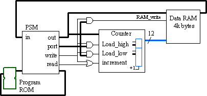
Registers can be used to compute start addresses from which data will be accessed (such as the beginning of text strings). This value is then loaded into the hardware address counter using a couple of output port locations. The hardware counter is then used to access the main data memory. As far as the PSM program is concerned, all reads and writes to the data memory occur at the same I/O port address. The added advantage of this technique is that the address counter can be made to increment automatically each time the PSM reads or writes information.
INNOVATIVE APPLICATIONS - These applications are innovative in their continued exploitation of the way in which a PSM is implemented inside the Xilinx FPGA. They build on the idea that there is now a software-programmable element inside a hardware-programmable device. The degree of flexibility that this offers is vast and is no longer limited to the larger and more costly devices. Now anyone with the most basic of Spartan-II evaluation boards may investigate these programmable options.
The most common observation is that the program for a PSM is stored in a block RAM. Typically, this is used as a ROM that is initialised by the configuration bit stream. This block RAM is, of course, RAM; therefore, the contents can be modified. The key factor here is that the memory is dual-port, which allows the PSM to read one port whilst the other is available to modify the code.
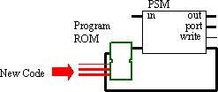
Although we could enter the scary world of self-modifying code, applications tend to be based on a completely new program being loaded into the memory for the PSM to execute. These may be the appropriate programs for handling different data types, protocols, or standards. This again means that the program space does not have to be very large and provides a method to support new protocols and standards in future.
Probably the most innovative concept is that of using the PSM as a sequencer. Each program becomes a one-shot event without the normal repeating loop. New execution sequences are then loaded into the program memory, possibly several hundred times per second. Since there would be so many different sequences to generate, and each sequence is by its very nature a sequential process, these sequences are much easier to develop in the software environment.
Thank you for following this series of articles -- I hope it has inspired you to either create your own programmable state machines or simply to use the ones that I have made available.
I have always found it interesting to study the implementation of a processor, as it consists of so many common digital logic building blocks. When memory, registers, multiplexers, adders, logical functions, and decoding logic can be efficiently implemented for a processor structure, it is a firm indication that similar techniques may be employed to implement virtually any digital function. It would be nice to think that you will also be able to exploit the Xilinx FPGA resources in similar ways in your own designs in future.
Although this is the last article of this series, please do continue to send me your e-mails to discuss this subject further, or simply to share your own PSM designs and applications of PicoBlaze (KCPSM) with me.
If you want to have a look at KCPSM (PicoBlaze), it is downloadable at the address below. (Full documentation and an assembler are also available for your use.) Over 1700 copies of KCPSM were downloaded from the web site in May, 2002.
XAPP213 "8-bit Microcontroller for Virtex Devices"
http://www.xilinx.com/xapp/xapp213.pdf
ftp://ftp.xilinx.com/pub/applications/xapp/xapp213.zip
This PSM is suitable for all Virtex, Virtex-E, and Spartan-II devices. If you would like a PSM specially tuned to the Virtex-II architecture, drop me an e-mail at ken.chapman@xilinx.com and I will be pleased to send it to you.
NOTE: Xilinx has recently given the KCPSM reference design the name "PicoBlaze," to indicate the complementary nature of the Programmable State Machines with the high performance 32-bit RISC soft processor called "MicroBlaze" that was released in October 2001. With PicoBlaze and MicroBlaze™, designers now can choose from a range of "right-sized" solutions, from 8 to 32 bits.
![]()
|
|
|
|