APPENDIX A. |
WORKED EXAMPLE: |
It is always instructive to learn from those who have gone before us. This appendix provides details of an FPGA-based prototyping project performed by a team in the Dallas DSP Systems division of Texas Instruments under the management of David Stoller. David is an applications engineer who has completed the RTL and systems verification of numerous IP modules and sub-systems integrated in cable and DSL modems, IP phones, and other networking-based products from Texas Instruments.
A1. Design background: packet processing sub-system
This case study examines the FPGA prototyping efforts within Texas Instruments of a complex packet processing sub-system as seen in Figure 169.
Figure 169: Packet processing sub-system block diagram (source: Texas Instruments)
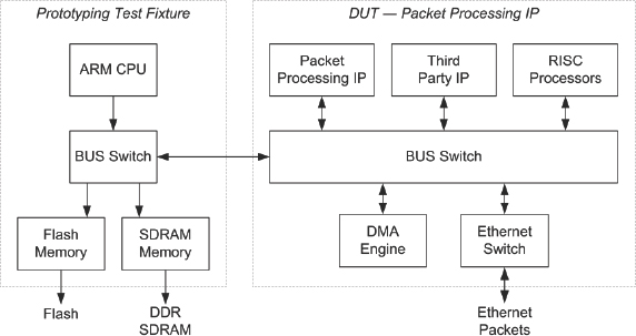
This particular sub-system consists of the following IP subcomponents each of which are tested individually or as part of the complete sub-system:
- DMA engine and packet-processing sub components
- Third-party IP
- 3-port gigabit Ethernet switch
- Firmware-based RISC processors
- Proprietary bus infrastructure
Within Texas Instruments, a typical IP design and verification cycle consists of the following steps:
- The IP design team defines the feature set of the IP to meet the application requirements, then specifies the IP and implements the design in RTL.
- The IP design team performs basic functional “smoke” testing to ensure that the RTL exhibits basic functionality.
- The IP design verification (DV) team then performs comprehensive simulation verification by implementing and running a large suite of test cases. When the IP is passing approximately 80% of the planned test cases, the design is considered robust enough for FPGA implementation.
- The IP prototyping team integrates the IP RTL into FPGA RTL, compiles the design for the targeted FPGA platform, and brings up the platform to begin FPGA testing.
- When the simulation and FPGA verification are complete, the IP module is released to the chip team, where it is integrated into the chip RTL.
- Chip-level verification is performed on the entire chip SoC through both SoC simulation verification and the use of a commercial emulator platform.
A2. Why does Texas Instruments do prototyping?
Each and every step in the design and verification flow is critical to the success of an IP block but the goal of the FPGA-based prototyping step is to perform pre-silicon verification of a complex IP block. FPGA-based prototyping allows the prototyping team to target conditions that are not easily replicated by alternate verification methods, including:
- Higher frequency RTL clocking, yielding very large numbers of test cycles.
- Memory transactions with real memory devices and other external peripherals.
- Networking protocol checking with actual networking equipment (USB, Ethernet, PCIe, etc.)
- Simultaneous interactions between multiple masters and peripherals or memory controller.
- Complete sub-system running at scaled clock frequency with heavy loading of interconnect buses to determine maximum throughput of logic and interfaces.
- Channel setup and teardown operations with and without traffic present.
- Testing IP running with actual asynchronous clock boundaries.
- Running real software applications which involve actual CPU instruction and data cache operations as well as management of peripherals through interrupt servicing.
Owing to the sheer number of gates present in the complete chip, the prototyping team did not intend for the FPGA prototyping platform to encompass the entire SoC. Instead, the primary goal was to map a part of the SoC that spanned 1-4 of the largest available FPGAs and could be run at approximately 10MHz. This allowed for a reasonable compromise between size and frequency to allow for useful FPGA prototype testing.
A3. Testing the design using an FPGA-based prototype
The IP DUT was tested by integrating the DUT RTL into an ARM® processor based sub-system which was then mapped onto the FPGA platform. This was previously illustrated in Figure 169.
The ARM processor served as the test host for the FPGA prototyping verification. Test applications written in “C” were run on the ARM to exercise the DUT with various scenarios that were defined in the FPGA test plan. In most cases, the memory map and infrastructure of the ARM sub-system were matched to that of the targeted chip. This allowed the FPGA platform to be used for software application and driver development before silicon was available. Additionally, having the FPGA test sub-system architecture match or resemble the architecture of the actual chip allowed for more meaningful performance measurements on the FPGA DUT.
The packet processing testing scenarios were broken up into two major classes.
Loopback tests were implemented by the ARM test application generating packets, sending them into the packet processing sub-system, receiving packets back from the hardware, and then checking the packets for data integrity. The packet loopback was performed at the boundary of the system (in the Ethernet PHY). Loopback tests were specifically designed for testing various packet configurations and extensive checking of all received packets through the ARM software.
Echo tests were implemented by sending packets from the Ethernet test equipment into the packet processing sub-system. The DUT routed the packets through its various hardware blocks, and then the packets were transmitted back to the Ethernet test equipment where they were checked for errors. Echo tests were specifically designed to maximize the packet throughput through the DUT, exercising the various parallel data paths, and provide minimal checking of errors among received packets.
Figure 170 provides an overview of the FPGA prototyping platform that was assembled for this project.
Figure 170: FPGA prototyping hardware used in the lab (source: Texas Instruments)
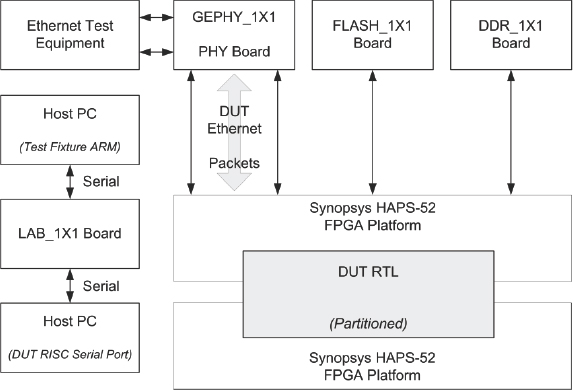
In this example, the DUT ARM processor executed a simple bootloader/OS out of flash memory in the same manner that the processor will on the final silicon. Test applications were loaded onto the flash or DDR SDRAM daughter board using either the serial port or ARM JTAG debugger on the LAB_1×1 board. The ARM executed the test application out of SDRAM and configured the DUT in preparation for running the tests. Ethernet packet streams were configured on the Ethernet packet generator which sourced them to the hardware platform on 10/100/1Gb interfaces to be processed by the hardware in echo tests. The Ethernet test equipment also served as a packet “checker” and verified that all expected packets were received, had no errors, and maintained the expected throughput rate.
A4. Implementation details
The entire packet processing RTL spanned four Xilinx® Virtex®-5 LX330 FPGAs (on two HAPS®-52 platforms or a single HAPS-54 platform). The final partitioning consisted of the following FPGA utilizations:
FPGA A 60% LUTs used
FPGA B 92% LUTs used
FPGA C 83% LUTs used
FPGA D 20% LUTs used
The FPGA implementation of the DUT was configured for two different clocking scenarios; “high-speed” and “low-speed” scenario.
The initial clock “high-speed” frequency targets were:
| Packet Processing IP: | 37.0MHz |
| Ethernet IP: | 12.5MHz |
| DDR SDRAM: | 50MHz |
Following the partition across 4 FPGAs using pin multiplexing techniques, the operating frequencies were lowered as follows in order to overcome some clocking limitations:
| Packet Processing IP: | 7.0MHz |
| Ethernet IP: | 12.5MHz |
| DDR SDRAM: | 50MHz |
Both scenarios yielded useful results and each shall be explained in detail, starting with the high-speed scenario.
A5. High-speed scenario
In order to properly test the packet throughput and pushback, specifically at the boundary between the 3-port gigabit Ethernet switch and the rest of the packet processing sub-system, it was necessary to set up the DUT to run at 1/10 of the clock speeds of the actual chip. By allowing the silicon clock ratio to be maintained on the FPGA platform, it ensured that each of the DUT components see the same level of transaction activity as the actual chip. For a silicon chip operating with a gigabit stream of Ethernet traffic running at 125MHz and the packet processing subsystem running at 370MHz, the corresponding FPGA-prototyped sub-system operated with a 100Mbit stream of Ethernet traffic running at 12.5MHz and the packet processing sub-system running at 37MHz.
Figure 171: Clocking structure for high-speed scenario (source: Texas Instruments)
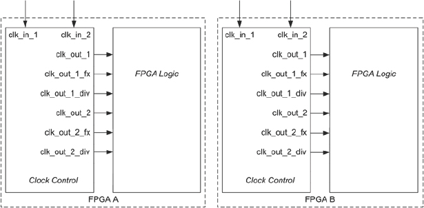
While this scenario satisfied the particular goal of testing the asynchronous boundary, it did present several challenges, including: FPGA interconnect pin limitations, FPGA capacity limitations, and the FPGA DCM minimum clock frequency. Both the interconnect and capacity limitations of the hardware platform drove a need for the platform to be implemented at these clock frequencies with a reduced DUT sub-system with some modules removed.
The clocks in this high-speed scenario were generated from a number of DCMs placed in the clock control block in Figure 171. However, by using the Virtex-5 DCMs to generate all of the required system clocks, the platform was limited to the combinations of clock division and phase shifting that could be achieved due to the 32MHz minimum clock input to the DCM.
This factor created issues with generating divided down or phase-shifted clocks which prevented certain IP modules from being included in this phase. Additionally, divided down clocks from the DCMs could not easily be used on multiple FPGAs, as it was difficult to ensure that they are synchronous and in phase.
A6. Low-speed scenario
The low-speed configuration was implemented in order to address the FPGA pin interconnect and capacity limitations of the hardware platform. By eliminating the requirement of implementing a packet processing IP/Ethernet IP clock ratio of 37/12.5, the FPGA RTL was reconfigured to include all of the DUT IP components (transitioning from two to four FPGAs) and to allow all of the resulting IP interconnect to be routed using the Synopsys® HSTDM pin multiplexing scheme.
Figure 172: Clocking structure for low-speed scenario (source: Texas Instruments)
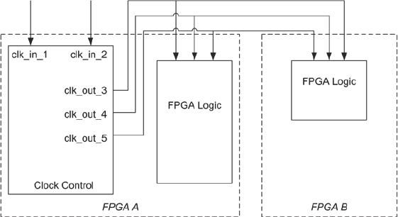
In order to resolve the limitations presented by the original clocking structure in the high- speed scenario shown above, the clocking structure in Figure 172 was implemented.
The low-speed clock scenario consisted of a central clock control module instantiated on one of the four FPGAs that generated all necessary system clocks using a simple FF counter clock divider scheme. This allowed the ability to generate unlimited divided and phase-shifted clocks from a single clock input fed through a DCM. These generated clocks were then fed out of the FPGA’s clock outputs, where they were routed back into each of the FPGAs on the platform.
This clocking structure had several advantages. First of all, this scheme allowed for a lower operating clock frequency that did not rely on the input requirements of the FPGA DCM. This low speed was necessary to implement pin multiplexing (HSTDM) between the FPGAs and therefore overcome any interconnect limitations. The low clock frequency also significantly reduced the FPGA synthesis and place & route runtimes. By having all of the generating clocks exit the FPGA outputs and then re-enter each of the FPGAs on their clock input pins, the FPGA compile tools could effectively ignore any of the clock generation circuitry in their analysis. This clock structure also provided much more flexibility when prototyping an IP that required a set of divided or phase-shifted synchronous clocks.
A7. Interesting challenges
The biggest challenges faced during the FPGA prototyping testing of the packet processing sub-system involved overcoming limitations of both FPGA capacity and FPGA pin interconnect.
FPGA capacity limitations were addressed by proper partitioning of the DUT RTL using manual methods as well as the Synopsys Certify® tool. This resulted in spreading out the DUT across two or four FPGAs. When done manually, this was a labor-intensive step which involved attempting various partitioning scenarios until the partition is successful. Using Certify eased much of the overhead involved in performing the complex partitioning.
FPGA capacity limitations were also addressed by constructing several configurations of the DUT RTL in which various sub-modules were removed in order to reduce the overall size of the sub-system. This was successful particularly when the IP contained several distinct functions, each of which could be separately tested. In some cases this allowed the DUT (with reduced resources) to be mapped across two FPGAs, allowing more efficient usage of multiple FPGA platforms by the team. However, this solution was entirely manual and added significantly to the time- and effort-resources spent on the FPGA implementation portion of the testing project.
When the packet processing RTL was partitioned across multiple FPGAs, there was often a conflict between how many pins were available between the FPGAs and how many were required by the internal signals within the DUT. Additionally, there was a trade-off between using the FPGA pins for external daughterboard connections and reserving the pins to accommodate FPGA-to-FPGA interconnect.
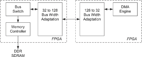
Initially, pin interconnect limitations were addressed by adding bus-width adapting bridges to internal buses within the DUT (i.e.128 bit adapted down to 32 bit). This solution shown in Figure 173, allowed for the FPGA operating frequencies of the sub-system to remain in the high-speed clocking scenario, although with a side effect, as it did modify the architecture (and possibly the functionality) of the DUT.
Figure 173: Block diagram of bus-width adaption (source: Texas Instruments)
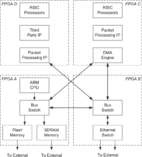
In order to implement and test the DUT without the presence of the bus width adaption bridges, the HSTDM pin multiplexing scheme within the Synopsys Certify tool was utilized. The HSTDM methodology was implemented using a 16:1 multiplexing ratio which allowed for all of the internal nets to be connected when the entire packet processing IP was partitioned across four FPGAs, as shown in Figure 174.
The trade-off with this methodology was that the HSTDM required a lower operating frequency and this was the overall driving factor in switching to the low-speed clocking scenario.
Figure 174: Block diagram of partitioned sub-system (source: Texas Instruments)
Summary of results
The FPGA-based prototyping team at Texas Instruments was able to construct a complete configuration of the packet processing sub-system and fully load it with multiple Ethernet streams to prove that the throughput and latency met the chip specifications. Once the DUT was up and running on the FPGA platform, hundreds of tests were run, uncovering multiple issues including several system-architecture problems that were impossible to replicate on a simulation or emulation platforms.
The FPGA platform was also used as a software development station for multiple engineers to perform software driver testing and firmware-based testing and development. The platform was operated in a time-sharing mode between the local hardware verification engineers and the remote software-verification engineers. Software engineers at a remote site were able to remote login to the host PC, which would allow them to access the ARM and RISC processor debuggers, to reset the platform when needed, and to perform their testing. They were able to load system-level tests and drivers onto the ARM processor and verify software applications prior to silicon being available.
Additionally, the software engineers were able to verify the firmware targeted for the various RISC processors in the packet-processing IP and demonstrate full functionality prior to silicon being available.
In addition to its hardware-verification advantages, the FPGA-based prototyping platform was demonstrated as a much more efficient software development platform than the emulator, providing a lower-cost solution, delivering many more test cycles and also having the ability to interface with a software debugger and real-time Ethernet test equipment.