APPENDIX B. |
ECONOMICS OF |
In chapter 5 and chapter 6 of this manual we explored the details of both making and buying a suitable FPGA platform. We tried to avoid making any value judgments between these two approaches because in any given situation one or the other may be most appropriate. This appendix is provided as a guide to help readers examine the business reasons for choosing between “make” and “buy.”
B1. Prototyping hardware: should we make or buy?
A wrong decision regarding the exact FPGA platform may have great impact on the cost and overall success of the whole prototyping project. The relative costs of various options might be the overriding consideration, but it is essential that the whole argument is considered. After all, if we have to compromise our prototyping goals to meet a budget, then let us at least be sure we understand all the cost factors involved.
The typical questions that arise when considering the best way to implement an FPGA prototype include “do I have enough time or expertise to create and manufacture a fully custom board?” or “will commercially-available boards cause me to compromise my goals too much?”
This section aims to expose the most significant factors to consider when choosing to develop or purchase prototyping hardware. Costs, development time, and effort are considered in detail; including the obvious direct factors of bill-of-materials (BoM) cost, manufacturing time and test yield as well as some related business issues, such as engineering opportunity cost, and return on investment (ROI).
Some time ago, the authors created a cost comparison spreadsheet (CCS) which is helpful in arranging all the cost and time factors involved. In the hands of a project manager in position of the ambient facts, the CCS allows us to explore the arguments based on our own situation. The references at the end of this book give details on how to obtain a copy of the CCS.
B2. Cost: what is the total cost of a prototyping board?
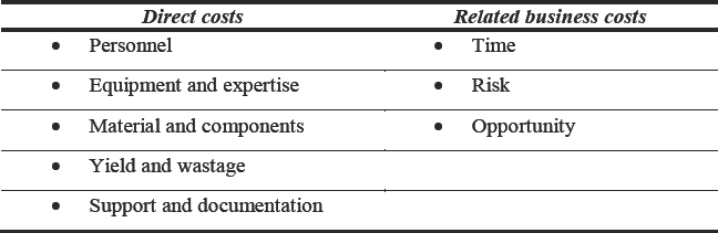
An FPGA-based prototype board is worth considerably more than the sum of its components. Comparison should not be made by simply comparing BoM cost of an in-house board vs. the purchase price of a finished commercial board. Many other costs beyond BoM should be amortized across the in-house board before cost comparison is made realistic. These costs can be grouped into direct and related business costs as shown in Figure 175. The following sections discuss each of these costs in depth.
Figure 175: Main costs associated with custom board development
B3. Direct cost: personnel
Design setup cost: prototyping requires specific FPGA expertise to perform set-up tasks which are independent of the target board, as explained in depth in chapter 7. Engineering effort will be expended on this kind of design manipulation regardless of our choice of board. A typical project might take four to six weeks to be set up by such experts. Using our CCS and entering typical data for engineering costs and overheads, we find that this set-up cost could typically be $20,000 per project (apologies to those reading in other countries but all cost examples in this appendix will be in $). For novice teams, the set-up time would be longer and costs would be proportionately higher.
Board engineering cost: there is an obvious difference in engineering cost between developing in-house boards and buying them ready-made. In the former case, the cost of development, manufacture and test must be borne by the project. In the latter case, it is the capital cost of buying in the board(s) that must be borne. Managers will understand that there is a difference between the visibility of project costs and visibility of capital costs at most corporations. Whereas the capital cost of purchasing ready-made boards is fairly obvious, the engineering cost of in-house development must also be fully understood in order to make an accurate comparison.
We must therefore have a figure for the development cost for the boards and then amortize this across the total number of boards in order to reach a per-unit development cost. To calculate a per-unit cost we should consider all relevant engineering costs, including:
- Development engineering
- PCB layout
- Manufacture engineering
- Test engineering
Once again, readers are urged to make calculations using their own figures; you will need to enter your company standard overhead and opportunity cost multipliers (e.g., overhead adds 50% cost on top of salary), and also estimate the time taken by each of the engineers to complete their tasks (e.g., PCB layout might take 40 days). The model used in the CCS includes these factors.
For example, 40 days is not unreasonable for a complex four-FPGA board with large BGA packages, trace-length matching, and 25+ layers. Using typical information entered into the CCS, cost for a 40-day PCB layout task may be estimated as $40,000, which is then amortized across the quantity of boards that are built and used in the project.
B4. Direct cost: equipment and expertise
General equipment is accounted for in the overhead multiplier on the personnel calculation above. However, in addition, there will be specific capital equipment employed to perform some of the design tasks. For example, a PCB layout station, manufacturing equipment, or test equipment. If there are production projects queuing up for the equipment while it is being used to create prototype boards, then there will be an opportunity cost associated with that. It is difficult to quantify that material opportunity cost and so they are not included in the CCS but you should consider where potential bottlenecks may be in your own capacity to design, build, and test boards.
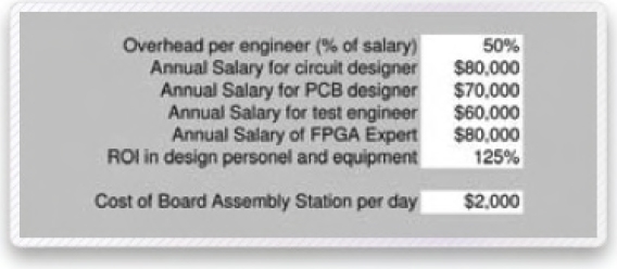
Figure 176: Engineering costs as entered into CCS
In the CCS, you can choose to factor equipment opportunity cost into the opportunity cost of the design personnel themselves. In any case, equipment opportunity cost should not be ignored. The CCS does, however, differentiate between in-house assembly costs and outsourced costs, including any non-recurring engineering (NRE) costs.
Engineering cost example
Figure 176 shows how typical data can be entered into the CCS. In this case we are making broad assumptions for salaries, overheads, and ROI. To clarify, the overhead of 50% means that for each dollar paid to the engineer, there is another 50 cents of extra cost (e.g., equipment, employment taxes, benefits etc.). The ROI figure attempts to model the opportunity cost; a figure of 125% means that the company would normally expect a return of 125 dollars of revenue for every 100 dollars paid in salary plus overhead for these engineers.
These figures are used for the calculations and for the purposes of this example are deliberately underestimating the real engineering costs. At risk of being repetitive, you may work with the CCS to enter your own information.
The engineering cost also depends upon how long these engineers are employed on the board development. We therefore have a section in the CCS in which we enter the estimated time required for the development.
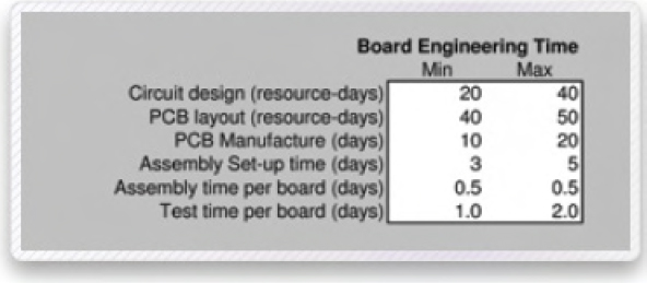
Estimates for time are difficult so we recommend using real data from a recent prototyping project rather than estimates for a future project. The CCS example in Figure 177 shows estimates based on real board designs known to Synopsys®. As is good practice for project management, there is a spread of estimates for each figure, which is given in resource-days. The CCS takes into account elsewhere how many engineers in each discipline are available for the project.
Figure 177: Estimates for engineering effort entered into CCS
We will see later how these figures impact the results of the CCS.
B5. Direct cost: material and components
Now that the board has been designed, it has to be built and this requires BoM management and component purchase effort. Simplistic analysis of “make vs. buy” decisions might only compare the component cost of the in-house board with the purchase price of the off-the-shelf board. As we have already seen, this ignores many significant costs.
Your own purchasing professionals will be very efficient in managing BoM costs for your own products in volume. This efficiency may not be fully transferable to very low volume runs such as prototyping boards. The extra effort to purchase and manage the BoM for a few FPGA-based prototype builds may not be a good use of their time or your component management system. The numbers are hard to measure but it is estimated by volume manufacturers that annual costs for maintaining items for production may be over $500 per different component type. When we consider that a four-FPGA board may have over 100 different component types, we can see that this becomes significant. This annual cost would be relevant if you are planning to use the boards in more than one project over a number of years. This is modeled as part of the board’s cost-of-ownership in the CCS. Regardless of cost, the extra time and effort involved in managing a BoM purchase compared to the purchase of a single off-the-shelf board is worth considering.
There are also economies of scale from which mass producers of commercial FPGA boards are able to benefit, resulting in lower prices for each final user. For example, the cost per device of the FPGAs will be lower to an external mass producer compared to buying them yourself in low-volume from your local distributor. In the CCS we can enter all material and component cost as a single overall sum which will then be used for other calculations.
Finally, for the bare-base PCB, assuming your manufacture is out-sourced, there will be a non-recurring engineering (NRE) or tooling cost for the board. In addition, the cost for the bare PCB is also significant enough for both to warrant separate entries in the CCS. As an illustration, a typical bare board cost for a four-FPGA board is approximately $2,000 in low volume with a further $2,000 to $3,000 NRE which should also be amortized.
Component and NRE example
We enter the approximate cost for the components including the PCB manufacture, the board itself, the FPGAs, and other components. The full BoM will be well understood for your own boards but for this example, we have estimated full component and board costs as shown in Figure 178.
Figure 178: Estimates for material costs entered into CCS
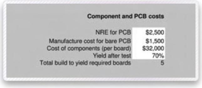
Total BoM price will vary depending upon the number of devices bought, minimum order quantities and discounts negotiated with vendors of the more important components on the board, for example the FPGAs and connectors. Of the $32,000 shown in our example, nearly half of that would be the cost of the four FPGA components themselves.
These components will need to be assembled onto the board and whether or not this assembly is performed in-house or contracted out, there is an associated cost to its setup. This may be an NRE at the external assembly house, or a less tangible in-house personnel/equipment cost. The CCS makes different calculations depending on your choice. In our example, we calculate an assembly cost per board of between $1,100 and $1,700 depending upon time during which in-house machinery is employed or external outsourcing is used.
These costs do not include board functional testing, which are accounted for elsewhere.
B6. Direct cost: yield and wastage
FPGA prototype boards are very complex and it is probable that the PCB design will require some rework, so the CCS takes account of possible re-spin costs and delays. Commercial board providers are able to amortize such re-spin costs over their entire production volume, whereas, in-house re-spin cost is borne by the awaiting SoC project.
In addition to board re-spin, it is also highly unlikely that there will be 100% yield of the boards after manufacture and assembly. Prototype boards are very sophisticated and have a large number of components and complex surface mount packages. Boards which do not initially work must have their failure diagnosed and remedial action must be taken. Automated production test methodology is often not economical for the very small volume builds and so the test and rework is usually performed by hand, often by the same experts that originally created the design. It is common to overbuild boards so that adequate boards pass initial test with minimal delay.
It is an unnecessary risk to build exactly as many boards as required and delay the prototyping project because engineers are occupied reworking the in-house boards rather than using the finished boards to verify the SoC. To put some figures on this, a typical yield after board population and initial test is 70%; so this is mitigated by building ten boards in order to quickly yield seven working boards. Commercial board vendors may have such rates for early production runs but they make incremental design and manufacture tweaks in order to remove recurrent faults, eventually raising the yield closer to 100%.
Additionally, the vendor has time for remedial rework on non-yielding boards as projects are not delayed and all boards will eventually be able to reach working stock. Finally, commercial board vendors have the production volume which allows more automation and faster yield to stock time. All yield improvement reduces wastage and cost.
We may find that delivery from working stock vs. bespoke manufacture and test is the most important differentiator in our make vs. buy discussion.
B7. Direct cost: support and documentation
One obvious way to reduce the above costs per board is to build enough boards so that they may be used for more than one project, thus reducing the cost per board per project. This may require a more flexible design and more robust fabrication in order to allow storage and re-deployment. Before the rise of today’s commercial board vendors, major users of FPGA prototyping had already built up their own internal board standards for reuse across multiple projects. Along with common hardware and interfaces made possible by this approach, the prototyping engineering expertise is also centralized and made available as a design service within the organization.
An extra task in such centralized organizations is the support and documentation of the boards for remote deployment. For example, the board may have been designed for use in an SoC project in the USA but reused for a quite different project by a team in Asia. Documentation must be adequate to allow such reuse and the original board designers should be available to support regular reuse as required. For this reason, it is normally only very large multi-national design teams that can afford such an investment in company-wide standards. Once established, prototyping teams may offer their valuable experience widely within their companies, however, it does not matter if the boards are developed in-house or sourced externally for this prototyping expertise to be valuable.
We have now considered the direct costs in producing or sourcing FPGA prototyping boards. Let us go on to discuss the previously mentioned business costs in turn. Some readers might say that these business costs are intangible and less under the control of Engineering department, however, they are often the deciding factor in the success or otherwise of a prototyping project.
B8. Business cost: time
How long does it take to design and make an FPGA prototype board? A typical 25 layer board with four large FPGAs in BGA packages, having maximum interconnect and necessary ancillary circuits (e.g., configuration and supervision functions) is a significant engineering challenge in its own right. Approaching this challenge with inadequate resources or insufficient experience often results in delay or failure; this is not a part-time job!
However, assuming we have the experience and sufficient access to the resources (e.g., PCB layout department) then we may estimate the time required. The estimate is broken into discrete tasks as follows:
Task 1: Circuit design
Task 2: PCB layout
Task 3: PCB manufacture
Task 4: Assembly set-up time including BoM purchase
Task 5: Assembly time
Task 6: Test time
Task 7: Rework time
Some of these tasks may be done in parallel, for example tasks 5, 6 and 7 would be like a “production” line with different boards at each stage at any one time. Other tasks are clearly sequential by necessity. It is also possible that task 4 might be started soon after task 1 is complete, assuming, of course, that the same people are not performing both tasks.
Allowing for parallel work, we arrive at the best-case project dependency shown in Figure 179.
Figure 179: Typical critical path for in-house board project
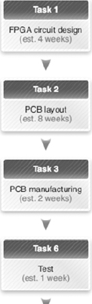
Once again, readers are encouraged to use their own in-house data, but for illustration, the authors are aware of typical design times of four weeks, PCB layout of eight weeks, manufacture two weeks, and test of one week. It is necessary to justify the PCB layout figure of eight weeks so let us consider this in particular.
High-performance FPGA prototyping boards are not simple. We are aiming to run very many traces between the FPGAs and other resources (connectors, memories etc.). The FPGAs are shipped in BGA packages with approximately 1,700 pins each, which lead to many thousands of traces being required on the board. It soon becomes apparent that a many-layered board is necessary which is pushing the limits of some automated PCB place & route tools. We also consider that, to maximize performance, clocks and resets must be cleanly distributed to all parts of the boards with minimal corruption or crosstalk. There is also the problem of delay matching on the board traces in order to balance the effect of signal distribution between FPGAs. Considering these criteria and other constraints, a layout in eight weeks is very reasonable.
Using the above approximations, we arrive at a best-case estimate of 15 weeks for in-house FPGA board development. How does this compare with a typical duration of an SoC prototyping project?
Analyzing survey data provided during users’ group meetings and dedicated on-line surveys, the authors have collated some typical information regarding the duration of FPGA projects. For example, Table 38 shows data summarized from a FPGA users’ survey performed in October 2007.
Table 38: Comparing prototyping and non-prototyping FPGA project durations
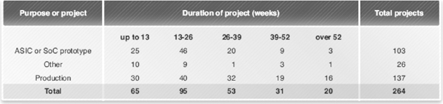
Within the granularity limits of this data, we can calculate that the average duration of a prototyping project is between 15 to 27 weeks. It is clear that the 15-weeks board development time estimated above does not fit well with our survey results. If the board were taken as the first task in a prototyping project, then the length of the project could double. If there are enough engineers available then board development and some of the design preparation can be performed in parallel. However, there is added risk if the board design is fixed before the SoC RTL is first mapped to FPGAs. We will consider this and other risks in the next section.
Example: time estimates
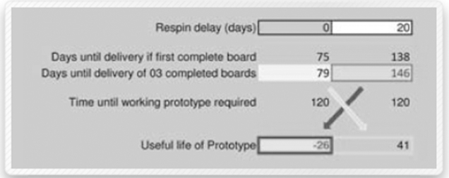
All of the above figures are used to calculate the cost but they also provide a coarse project timeline. Of course, the CCS must only be used as a rough rule-of-thumb before entering into proper timeline analysis as part of correct project management. In Figure 180 we see the CCS time estimates based on all the above data entered for our example. The spread of best-case and worst-case results is very wide.
Unfortunately, the time allowed for completion of the prototype project is a constant. In our example, we can already see that if the project is started with in-house board development, then the useful time for actually using the prototype to verify the SoC can quickly disappear. In this example, there is a risk that the boards will not be available until well after the planned end of the project.
Figure 180: Comparison of estimated useful lifetime of boards (from CCS)
B9. Business cost: risk
The aim of our FPGA-based prototyping methodology is to reduce risk in an SoC project; therefore we should not be adding further risk or delays by cutting corners on verification.
Delays in the prototype causes delays in the SoC verification overall and/or delay in the SoC sign off and follow-on delays in the product’s final introduction. It is widely accepted that release postponement will reduce a product’s total revenue in the end-market so risk is counted as a related business cost in this section i.e., raised risk means that market-reducing delays are more likely to happen.
For this analysis we will compare the risk in building in-house boards vs. buying off-the-shelf. For example, delays may occur because of limited supply of off-the-shelf boards or because of a longer than expected development or manufacture time of in-house boards. On the other hand, external board suppliers must also be able to deliver to their quoted schedules so this is not a one-sided consideration. Let us consider how risk might be reduced.
Excess capacity reduces risk: let us continue the previous discussion about saving time by designing the board and preparing the SoC design in parallel. It is possible that the FPGA capacity or interconnect requirements might be incorrectly estimated too early in the project; for example prior to partitioning. Of course the SoC design itself may also change as the SoC project matures but this would be a risk in either the in-house board or off-the-shelf board. More realistic estimates would yield even higher per-project costs for the in-house boards.
The risk in starting the in-house FPGA board design early may be mitigated by making the board design as flexible as possible. This contradicts the natural temptation to design the board with topology to match the top-level blocks of the SoC, e.g., “this big block in that big FPGA; this smaller block in that smaller FPGA.”
Instead, we should try to provide some margin in the available FPGA resources on board. A good rule of thumb is to place twice as much FPGA resource on the board as the initial synthesis and place & route runs suggest. Skimping on the FPGAs used is a false economy compared the increased risk placed into the SoC project by doing so.
Interconnect flexibility reduces risk: the interconnect traces between the FPGAs should be ample and general rather than guided by the top-level signal buses in the SoC design. Top-level design interconnect can change if new top-level functions are added to the design so the board-level interconnect must be able to follow suit. If it cannot, then unnecessary project delay may occur while a new partition of the design is found, perhaps requiring that signals be multiplexed onto the same interconnect.
Whether or not the interconnect resource needs to be performed remotely using programmable links, or locally and manually altered by using physical connectors, depends on the requirement for the boards. If it is to be used almost simultaneously for multiple projects, perhaps like some kind of “prototyping farm,” then it would need to be remotely programmable, probably using some kind of in-line signal switching between FPGAs.
Alternatively, it may be that the platform will be configured once per project with the right FPGA resources with the interconnect established and the necessary peripherals in place. In this case, the interconnect “switching” can be manual which simplifies the board design and may allow higher performance.
Peripheral de-coupling reduces risk (and increases reuse): as mentioned previously, in-house boards may be designed for a single project or might be expected to be used across multiple projects. In the former case, it is tempting to place all the necessary hardware peripherals needed to match the functions instantiated inside the SoC, for example, the RAM, PCI, video, and co-processor cores in chip form, mounted and connected into the board in the same way that they are in the SoC. The risk introduced is the same as for the capacity and interconnect cases mentioned above. If the SoC topography or peripheral content is changed (for example, a second PCI port is added) then it may take many weeks to rework the board to add the new function. A modular approach is clearly advisable, so that daughter cards may be mounted on the main FPGA boards in order to provide the necessary extra peripheral functions.
Those expert teams providing many in-house boards across multiple projects universally adopt a modular arrangement of motherboards and separate peripherals which may be designed quickly and with less error.
If the peripheral boards are connected together with a motherboard using a standard connector arrangement then this greatly increases the options for their reuse in other projects. Some commercially available FPGA prototyping systems follow this modular approach as well and have built up a large selection of optional peripheral functions available as daughter boards. This allows us to select and assemble the required resources for the project and then reassemble and augment for the next project. This also reduces the risk that late changes in the SoC design cannot be quickly accommodated by the prototype board.
Expert advice reduces risk: if this is your first prototyping project, then it is advisable to employ an external consultant or allocate your best staff FPGA experts to help with SoC design preparation. They will be able to give early appraisal of the necessary resources, interconnect, and flexibility required and ensure that late project changes do not render the entire prototype unusable. They should not only be able to provide high-quality guidance to the FPGA board designers, but also appraise whether commercially available boards will meet the project requirements.
B10. Business cost: opportunity
Having considered time and risk, we should also include the opportunity cost for developing boards in-house. Opportunity cost can be defined as that benefit which has not been realized elsewhere because resources (i.e., engineers in this case) are allocated to a given project. In the CCS, opportunity cost is expressed as a missed ROI. You can enter the normally expected revenue (or other output) generated by the engineers as a percentage of their cost. For example, each engineer may otherwise generate $2.00 of final revenue for each $1.00 of cost (i.e., salary etc.) resulting in an ROI of 200%. This is realistic because design of FPGA prototype boards takes a great deal of FPGA design expertise which would also be very valuable elsewhere.
B11. CCS worked example results
Given the variables and constants we have used in our example throughout this section, the main result from the CCS will be the cost comparison. The result panel for the CCS is shown in Figure 181.
The cost is either per board, such as test, or per project, such as the PCB layout which then has to be amortized across the total number of boards in order to arrive at a per board amount; obviously, the larger the number of boards, the smaller the cost of each board. Commercial board vendors can take advantage of this “economy of scale” and to pass on these economies to customers. We should expect that for low volumes, it is cheaper to buy boards than to make them in-house.
Figure 181: Design example cost results given by CCS
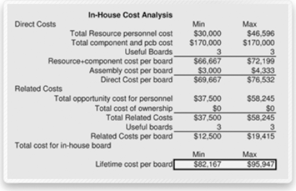
The example prototyping project calls for low volume (only three boards) and with the previously mentioned costs, we see that the best-case cost for each board would be around $82,000 or as much as $96,000 if it took a little longer for each task and a PCB re-spin was required. We have purposely used low estimates and values in this example; more realistic estimates would yield even higher per-project costs for the in-house boards.
If you work with a spreadsheet like the CCS or a much more sophisticated project management tool, you can alter any of the variables to see what effect this will have on the real board costs. However, it is important to keep the board cost in perspective to the other costs and risks and how that fits into the overall SoC project timescales.
B12. Summary
For any given project there is a threshold of board volume beyond which it will be more economical to make boards in-house. Beyond the economic arguments there may be technical merit in making boards in house, for example to meet a certain form factor or topology requirement. Using a spreadsheet like the CCS, we can be sure to expose all the cost and timescale implications but the technical requirements, as explored during this chapter, may be a deciding factor. Most important of all, in the end, is time. It is critical to FPGA-based prototyping that the SoC project does not depend upon early delivery of new in-house boards.
Generally, the minimum-risk approach does not involve making boards in-house, however, the alternative of finding the right commercially available boards to meet the same need in doing so may be very high.