CHAPTER 1 |
INTRODUCTION: THE |
This chapter will establish some definitions and outline the challenges we are trying to overcome with FPGA-based prototyping. We will explore the complexity of SoC-based systems and the challenges in their verification. We will also compare and contrast FPGA-based prototyping with other prototyping methods including system-level virtual modeling. After this chapter we will be ready to dive deeper into the ways that FPGA-based Prototyping has benefited some real projects and give some guidance on what is possible with FPGA-based prototyping technology.
1.1. Moore was right!
Since Gordon E. Moore described the trend of how many transistors can be placed inexpensively on an integrated circuit, electronic design enabled by semiconductor design has grown at a hard-to-imagine pace. The trend of transistors doubling every two years has already continued for more than half a century and is not expected to stop for a while despite repeated predictions that it would end soon.
A detailed review of the major trends driving chip design later in this chapter will make it clear why prototyping has grown in adoption, and is even considered mandatory in many companies. To further understand this trend, typical project dynamics and their effort distributions need to be understood.
1.1.1. SoC: A definition … for this book at least
Let’s start with a definition. For the purposes of this book, we define system on chip (SoC) as a device which is designed and fabricated for a specific purpose, for exclusive use by a specific owner. Some might think of SoC as a particular form of an ASIC (application specific integrated circuit) and they would be correct, but for the purposes of this book, we will refer only to SoCs. We will stick to the definition that an SoC always includes at least one CPU and runs embedded software. In comparison, an ASIC does not necessarily include a CPU and to that extent, SoCs can be considered to be a superset of ASICs.
We do not mean to imply that those who are creating an ASIC, ASSP (application-specific silicon product) or silicon produced by COT (customer’s own tooling) or by third-party foundries should read another book. Technologies are not mutually unique for FPGA-based prototyping purposes and in fact, many FPGA-based prototyping projects are of an ASSP or even just pieces of IP that may be used in many different SoC designs.
As far as FPGA-based prototyping is concerned, if it works for SoC then it will work for any of the above device types. The reason for this book’s focus on SoC is that the greatest value of FPGA-based prototyping is in its unique ability to provide a fast and accurate model of the SoC in order to allow validation of the software.
1.2. The economics of SoC design
SoC designs are all around us. We can find them in all the new headline-grabbing consumer electronics products as well as in the most obscure corners of pure research projects in places like CERN, and in the guidance systems of interstellar probes.
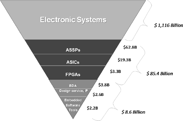
Figure 1: The relationship of IC design to the electronics market
For consumer products in particular, there is a seemingly insatiable hunger for maximum intelligence and functionalities in devices such as smart phones, cameras or portable media players. To meet these requirements a typical SoC design will include several microprocessors, one or more digital signal processors and some different interfaces such as Bluetooth™ or WLAN, high resolution graphics and so on. That all adds up to a lot of software.
Considering the IC development and manufacture as a whole, it appears in Figure 1 as an inverted triangle. The figures shown are for 2009, and we see that chip development was a market of about $85.4 billion and was enabled by a $8.6 billion market for EDA tools, design services, IP and embedded software tools. Supported by this semiconductor design and manufacture is a huge $1.116 billion market for electronic systems, which contain for example all the consumer gadgets, wireless devices and electronics we crave as end consumers.
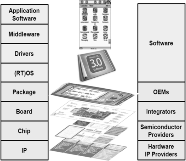
Figure 2: Hardware-software teardown of a consumer device
EDA tools, which include various types of prototyping for different stages within a design, are recently focusing to specifically enabling the design chain from IP providers, semiconductor providers, integrators and OEMs. Prototyping plays a key role in those interactions as early prototypes enable communication of requirements from customers to suppliers and early software development and verification for customers from suppliers.
To understand the impact that prototyping in its many forms can achieve, let’s consider a typical complex SoC design. Figure 2 shows the tear down of a typical smartphone. The end user experience is largely influenced by the applications with which they are presented. Good old hardware, analog and antenna design is obviously still important but the user only really notices them when they go wrong! User applications are enabled by a software stack of middleware, operating system and drivers; all of which are specifically design to make the software as independent of the hardware as possible.
For example, application developers do not have direct access to the device’s hardware memory, timing or other low-level hardware aspects. The stack of software is matched by a stack of hardware elements. The end device uses several boards, comprised of several peripherals and chips, which contain various blocks, either reused as IP or specifically developed by chip providers to differentiate their hardware.
The dependencies of hardware and software result in an intricate relationship between different company types. IP providers sell to semiconductor providers, who sell to integrators who sell to OEMs, all of whom are enabling software developers. Enablement of these interactions has arguably become the biggest problem to be addressed by tool vendors today.
The main challenges for this enablement have become today:
(a) The enablement of software development at the earliest possible time.
(b) Validation of hardware / software in the context of the target system.
(c) Design and reuse of the basic building blocks for chips
- processors
- accelerators
- peripherals
- interconnect fabrics (e.g., ARM AMBA® interconnect)
(d) Architecture design of the chips assembled from the basic building blocks.
1.2.1. Case study: a typical SoC development project
Considering the bottom three layers of the hardware stack in Figure 2, let’s analyze a specific chip development project and the potential impact of prototyping. The chosen example is a wireless headset design by a large semiconductor company, performed in a mainstream 65nm technology. The chip is targeted for a high volume, fast moving market and has an expected production run of 27 months with an average volume of 1.5 million units per month and average selling price of $5.50. Things go well during development and only one metal mask spin is required allowing six months of customer and field evaluations after first silicon is available. In total the development cost for the project is estimated as $31,650,000 based on a development cost model described in an International Business Systems study with scaling factors for mainstream applications.
Let’s now consider Figure 3, which illustrates how chip development cost is spread over the typical 12-month hardware design cycle, from complete specification to final verified RTL, ready for layout. Indeed, RTL verification consumes the majority of the effort and is the critical element in determining the project length of 12 months. Another portion of the design with significant impact is the overall design management accompanying the actual development of code. Physical design is finished about 15 months into the project (i.e., three months after RTL is verified) and then masks are prepared by month 17. The post silicon validation ramps up with engineering samples available in month 19 and takes several months.
Figure 3: Project effort for a 65nm wireless headset design
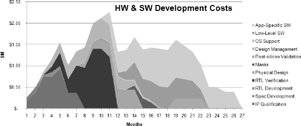
As Figure 3 further illustrates, software development ramps up in this project when RTL is largely verified and stable. It is split here between OS support and porting, low-level software development and high-level application software development. All the software development effort here is still the responsibility of the chip provider, rather than third-party providers. Overall, software development consumes 40% of the total cost for this design and extends the project schedule to a total of 27 months.
When amortizing development and production cost onto expected sales, this project reaches break even after about 34 months, i.e., seven months after product launch but almost three years after starting product development. The challenge in this example is that we have to predict nearly three years in advance what is going to sell in high-volumes in order to specify our chip. How can this almost intolerable situation be made easier? The answer is to “start software sooner.”
Using the calculator for return on investment (ROI) developed by the Global Semiconductor Association (GSA), it can be calculated that if software development and validation started seven months earlier in our example project, production could have started three months earlier and subsequently the time to break even would have been reduced by five months. In addition a $50 million revenue gain could have been expected over the production volume due to extra first-to-market design-wins for the chip.
This is exactly what prototyping in its many forms can achieve. The earlier start to software development and validation provided by prototyping means that its impact on ROI can be very significant.
For a deeper understanding of requirements and benefits of prototyping, let’s look at the different types of prototyping available today from virtual to FPGA-based.
1.3. Virtual platforms: prototyping without hardware
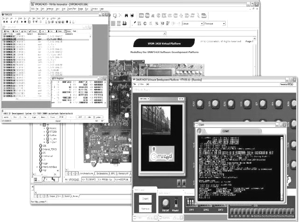
There are various forms of prototyping which we can employ in our projects. Available earliest in a project are virtual prototypes. They represent fully functional but loosely-timed software models of SoCs, boards, virtualized IOs and user interfaces, all running on a host-based simulation. Virtual prototypes can execute unmodified production software code on processor instruction set simulators and they run close to real-time. Being fully host-based virtual prototypes they can also offer good system visibility and control, which is especially useful for debug on multicore CPUs. Virtual prototypes can also have virtual user interfaces, allowing real-time interaction with us slow humans. The screenshot excerpts shown in Figure 4 are from a virtual prototype of an OMAP design running on the Synopsys Innovator tool. Here we see not only recognizable simulation windows but also the representation of key controls on the board and input from a virtual camera, in this case linked to a webcam on the host PC running the simulation, all done without hardware. We shall come back to Innovator in chapter 13 when we discuss the linking of an FPGA-based prototype with a virtual simulation.
While virtual prototypes offer very high speed (multiple tens of MIPS) when using loosely-timed models they do not offer the timing accuracy preferred by hardware design teams. More timing-accurate software models can be added to a virtual prototype but then their simulation speed will degrade to the single-digit MIPS range or even lower depending on the mix of cycle-accurate versus loosely-timed models.
However, virtual prototypes are available earliest in the flow, assuming models are available, so they are perfect for early software debugging. Virtual prototypes provide almost complete insight into the behavior of the system and they are also easy to replicate for multiple users.
Figure 4: Pre-Silicon virtual prototype of OMAP design
Finally, because they are created before the RTL, virtual prototypes allow co-development of hardware architecture along with early software. For example, extra or different CPUs might be added if the virtual prototype shows that there is not enough processing bandwidth for the product’s concurrent applications.
1.3.1. SDK: a very common prototyping environment
Related to virtual prototypes are so-called software development kits, or SDKs, of which a very common example is the SDK for developing applications for the Apple iPhone®. This SDK was downloaded more than 100,000 times in the first couple of days of its availability and so we can consider this a very widely available prototyping platform. Although simple in comparison, SDKs offer many of the advantages of full virtual prototypes, however, their accuracy is often more limited because they may not represent the actual registers as accurately as virtual prototypes.
Their aim is to have “just enough accuracy” in order to fool the application into thinking that it is running on the final platform. SDKs allow programming and interfacing over a higher-level application programming interface (API) into the platform. The developed software is usually compiled for the host machine on which the SDK executes and then requires re-compilation to the actual target processor after programmers have verified functionality on the SDK.
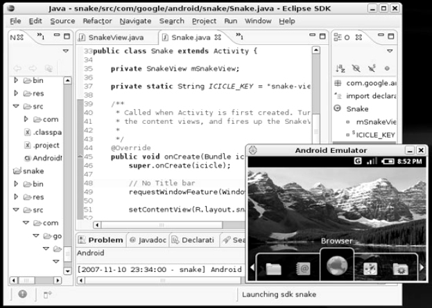
Figure 5 shows a screenshot of an Android™ SDK. Programming of applications is done in high-level languages like C using higher-level operating system APIs. The programming is done completely independent of the actual target hardware, so when actually targeting the final device, recompilation is necessary. User interfaces of the target device – as shown in Figure 5, can be modeled so that the end-user environment can be experienced virtually.
Figure 5: Android™ SDK screenshot showing GUI emulation
1.3.2. FPGA: prototyping in silicon … but pre-silicon
Available later in the design flow, but still well before real silicon, an FPGA-based prototype also serves as a vehicle for software development and validation. FPGA-based prototypes are fully functional hardware representations of SoCs, boards and IOs. Because they implement the same RTL code as the SoC and run at almost realtime speed with all external interfaces and stimulus connected, they are very accurate. They offer higher system visibility and control than the actual silicon will provide when available but do not match the debug and control capabilities of virtual platforms, or any other simulator, so they are not the first platforms we would choose on which to debug all of our RTL.
The key advantage of FPGA-based prototypes is their ability to run at high speed, yielding tens of MIPS per modeled CPU, while maintaining RTL accuracy. They are typically available later in the design flow than virtual prototypes because RTL needs to be available and relatively mature. Due to the complexity and effort of mapping the RTL to FPGA-based prototypes, it is not really feasible to use them before RTL verification has stabilized. For the same reason, FPGA-based prototypes are not intended for use as hardware/software co-development platforms because at this point in the SoC design flow, the hardware (i.e., the RTL) is pretty much fixed and partially verified. Design teams will be very hesitant to change the hardware architecture by the time the FPGA-based prototype is running, unless some major architectural bottlenecks have been discovered.
Finally, once stable and available, the cost of replication and delivery for FPGA-based prototypes is higher than for software-based virtual platforms, however still considerably cheaper than emulators, which we shall discuss next.
1.3.3. Emulators: prototyping or verification?
Emulation provides another hardware-based alternative to enable software development but differs from FPGA-based prototyping in that it aims at lower performance but with more automation. Emulators have more automated mapping of RTL into the hardware together with faster compile times, but the execution speed will be lower and typically drop to below the single-MIPS level. The cost of emulation is also often seen as a deterrent to replicating it easily for software development despite the fact that emulators are popular with software engineers because of their ease of use.
As with FPGA-based prototypes, emulators are not realistic platforms for hardware-software co-development because they require the RTL to be available. A more likely use for emulators is as an accelerator for normal RTL simulation and so many consider emulation not as a prototyping platform but as an extension to the normal verification environment; a kind of go-faster simulator. An emulator can actually be used for software development, however, only when the software needs cycle-accuracy and high-visibility into the RTL and can tolerate very slow run speed. Software would need to be limited to short duration runs, such as the boot ROM code, because the slow running speed will mean that runtimes can be very long; certainly too long for long software tasks, such as user applications or OS bring-up.
1.3.4. First silicon as a prototype platform
Finally, after the actual silicon is available, early prototype boards using first silicon samples can enable software development on the actual silicon. Once the chip is in production, very low-cost development boards can be made available. At this point, the prototype will run at real-time speed and full accuracy. Software debug is typically achieved with specific hardware connectors using the JTAG interface and connections to standard software debuggers. While prototype boards using the actual silicon are probably the lowest-cost option, they are available very late in the design flow and allow almost no head start on software development. In addition, the control and debug insight into hardware prototypes is very limited unless specific on-chip instrumentation (OCI) capabilities are made available. In comparison to virtual prototypes, they are also more difficult to replicate – it is much easier to provide a virtual platform for download via the internet then to ship a board and deal with customs, bring-up and potential damages to the physical hardware.
As can be seen by this overview, prototyping is focused on providing early representations of hardware, specifically of chips and their surrounding peripherals. Prototypes are applicable for different use models, which in exchange have an impact on requirements.
1.4. Prototyping use models
As indicated earlier, prototyping is done today using different execution engines. Once a chip development project has started, project managers are asked almost immediately to provide early representations – prototypes – of the “chip-to-be” for various purposes, such as:
- Marketing needs material and basic documentation to interact with early adopters.
- Software developers would like executable representations of the design under development to allow them to start porting operating systems
- Hardware developers would also like executable specifications to validate that their implementations are correct.
- Prototypes are in high demand from day one! The need is driven by three main use models: architecture exploration, software development and verification.
1.4.1. Prototyping for architecture exploration
At the beginning of a project, architecture exploration allows chip architects to make basic decisions with respect to the chip topology, performance, power consumption and on-chip communication structures. For example, information gathered early on cache utilization, performance of processors, bus bandwidth, burst rates and memory utilization drives basic architecture decisions.
In an ideal world, chip architects would love to get prototypes with fully accurate models – representing all internals of the design – while running at full speed. Unfortunately, both characteristics typically cannot be achieved by the same model. Fully accurate data cannot be gathered until the final chip comes back from fabrication or at least until late in the design cycle, when RTL is available and verified. At that point, FPGA prototypes can be used to execute the design close to real time.
Chip architects also interact with “early adopter” customers and ideally would like executable specifications to demonstrate key features of the design. However, in reality, chip architects mostly rely on tools like Microsoft Excel™ for basic, static architectural analysis. Often they have to rely on their experience and back of the envelope assessments. As a result, interaction with early adopter customers happens based on written specifications and lots of joint discussions at white boards.
1.4.2. Prototyping for software development
Software developers would ideally like to start their porting of legacy code and development of new software functionality from the get go, i.e., when the hardware development kicks off. They would like to receive an executable representation of the chip, which runs at real-time and accurately reflects all the software related interfaces with the hardware (like register images). Depending on the type of software being developed, users may require different accuracy from the underlying prototype. The type of software to be developed directly determines the requirements regarding how accurately hardware needs to be executed:
- Application software can often be developed without taking the actual target hardware accuracy into account. This is the main premise of SDKs, which allow programming against high-level APIs representing the hardware.
- For middleware and drivers, some representation of timing may be required. For basic cases of performance analysis, timing annotation to caches and memory management units may be sufficient, as they are often more important than static timing of instructions when it comes to performance.
- For real-time software, high-level cycle timing of instructions can be important in combination with micro-architectural effects.
- For time-critical software – for example, the exact response behavior of interrupt service routines (ISRs) – fully cycle-accurate representations are preferred.
Often still today, developers will start software development “blindly,” based on register specifications, but are then plagued by not being in sync with changes the hardware team still may make to the register specifications. For derivative product families, application software is often developed using high-level APIs, which can be executed on a previous generation chip. The underlying drivers, OS and middleware, which become available later, make sure that the APIs remain the same and do not break legacy software.
1.4.3. Prototyping for verification
Early on, the chip environment is represented using traces and traffic generators. Early test benches essentially define the use model scenarios for the chip under development.
In a typical design, just as many bugs hide in the test bench as in the actual design itself. Therefore, it is important to start with the development of test benches for verification as early as possible. Ideally, verification engineers would like an executable representation of the “device under test” (DUT) to be available from the start. Similar to software development’s need for different models, verification has requirements for different levels of accuracy as well.
High level models of the DUT will enable development of verification scenarios. Models of the DUT with accurate registers and pure functional representation of the DUT’s behavior satisfy a fair share of test bench development. For verification of timing and detailed pipeline latencies, timing approximation may initially be sufficient but eventually a cycle-accurate representation at the register transfer level (RTL) will be required.
An important trend in hardware verification is the move of functional verification into software, which executes on processors embedded in the design. In answer to the recent survey question “Do you use software running on the embedded processors in your design for verification of the surrounding hardware?”, more than 50% of the respondents answered that they are already using embedded software for verification, and one in ten of them also use it with a focus on post-silicon validation.
The advantage of this CPU-based approach is verification reuse:
- Tests are executed on processors and developed initially using fast instruction-accurate processor models interacting with transaction-level models (TLM) of the DUT, accessing it through its register interface.
- Later the tests can be reused in mixed TLM/RTL simulations as well as in pure RTL simulations for which the processor is mapped into RTL.
- The tests can still be used for hardware prototypes with the processor executing as TLM on the workstation, connected to the hardware via highspeed TLM interfaces.
- Processors executing the tests can also run as RTL in the FPGA prototype or can be brought as chip on a plug-in board into the FPGA prototype.
- Finally, when the chip is back from fabrication, software-based tests can be used for post-silicon verification as well.
1.5. User priorities in prototyping
With all of those trends combined, prototyping of chips is becoming a clear requirement for successful chip design. However, different user priorities lead towards different prototyping options as the best solution. We can list them in a number of ways but in our case, we chose to highlight twelve different priorities, as listed below.
- Time of availability: once the specifications for our design are frozen, delays in delivery of our software validation environment directly impacts how quickly we can start and progress in the software part of our SoC project.
- Execution speed: ideally the chosen development method provides an accurate representation of how fast the real hardware will execute. For software regressions, execution that is faster than real-time can be beneficial.
- Accuracy: the type of software being developed determines how accurate the development methods have to be in order to represent the actual target hardware, ensuring that issues identified at the hardware/software boundary are not introduced by the development method itself.
- Capacity: can the prototype handle the largest SoC designs or is it not required to do so? How does performance and cost alter with increased design size? Can the platform be upgraded for larger designs in the future?
- Development cost: the cost of a development method is comprised of both the actual cost of production, as well as the overhead cost of bringing up hardware/software designs within it. The production cost determines how easy a development method can be replicated to furnish software development teams.
- Bring-up cost: any required activity needed to enable a development method outside of what is absolute necessary to get to silicon can be considered overhead. Often the intensity of the pressure that software teams face to get access to early representations of the hardware determines whether or not the investment in bring-up cost is considered in order to create positive returns.
- Deployment cost: if we are to create multiple copies of our prototype then we need to be aware of how much each will cost to create, deploy, maintain and support in the labs of our end users and beyond.
- Debug insight: the ability to analyze the inside of a design, i.e., being able to access signals, registers and the state of the hardware/software design.
- Execution control: during debug, it is important to stop the representation of the target hardware using assertions in the hardware or breakpoints in the software, especially for designs with multiple processors in which all components have to stop in a synchronized fashion.
- System interfaces: if the target design is an SoC, it is important to be able to connect the design under development to real-world interfaces. For example, if a USB interface is involved, the software will need to connect to the real USB protocol stacks. Similarly, for network and wireless interfaces, connection to real-world software is a priority.
- Turnaround time: from a new set of source files, be they SystemC™ models or raw RTL, how long does it take to create a new version of the prototype? Is it measured in minutes, hours, days or weeks and what is required for the project in any case?
- Value links to low power and verification: prototypes do not have to be stand-alone platforms and it may add value if they can be linked to other parts of the SoC design team, particularly for verification. Prototyping before and after insertion of various implementation steps, for example modifications to reduce power, would also be valuable.
Probably no user has ever cared about all of these decision criteria at the same time and for any given SoC project, some will override others. We shall revisit most of these criteria as we progress through this book.
At the end of the book we will look to the future of prototyping as a whole and the place of FPGA-based prototyping in that future. On looking to the future we need to be aware of the recent past and trends that are emerging within the SoC user-base and wider industry. Let us look at those trends now.
1.6. Chip design trends
We will want to use our prototyping environment for future SoC projects but what will those projects look like? Understanding the eight major trends for chip design will lead to better readiness for future projects and a more flexible in-house prototyping methodology.
The eight major trends driving requirements for semiconductor design are:
- Further miniaturization towards smaller technology nodes.
- A decrease in overall design starts.
- Programmability combined with a rapid increase of embedded software content.
- IP reuse.
- Application specificity.
- Adoption of multicore architectures.
- Low power.
- An increase in the analog/mixed signal portion of chips.
All of these have profound impact on prototyping requirements and we shall quickly look at each and the supporting trend data in turn.
1.6.1. Miniaturization towards smaller technology nodes
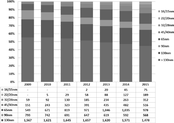
In processor design the number of transistors has increased from 29,000 transistors defining the X86 in 1979 to 1.72 billion transistors by 2005 defining the Dual Core Itanium. That was an almost 60,000 fold increase over the time frame of 26 years. This trend has continued since and is likely to continue in the future and the number of design starts at smaller technology nodes will increase as outlined in Figure 6. This diagram (courtesy of the industry analyst, International Business Strategies Inc. (IBS) of Los Gatos, CA) shows each node as a percentage of all ASIC and SoC design starts.
Designs at the 65nm and 45nm nodes started in 2007 and have now become mainstream. As a result the size of designs to be prototyped has steadily increased, requiring more and more capacity for both software- and hardware-based prototypes.
Software-based prototypes are naturally limited in speed by the traditional serial execution of software. This has further increased the pressure to improve the speed of software simulation, especially for processor models.
Figure 6: Design starts per technology node (Source: IBS)
While fast simulation models have been available since the late 1990s using proprietary techniques, standardization has now enabled the combination of models from various sources into SystemC-based simulations without significant speed degradation using the open TLM-2.0 APIs.
For hardware-based prototypes this trend has further increased the pressure to adopt higher-density FPGAs for prototyping. Given that the capacity of FPGA prototyping is limited by the capacities of the available FPGAs, the only alternative is to divide and conquer and to only prototype smaller parts of the designs. To address this situation, FPGA prototypes have become more scalable using standard interfaces for stacking and expansion. Finally, in situations in which a prototype is to be tested within the system context of the chip under development, partitioning of the design can be difficult. Given that the number of FPGAs per prototyping board will increase to allow for sufficient capacity, the requirements on automatically partitioning the design across FPGAs has also increased.
1.6.2. Decrease in overall design starts
On the flip side of the trend towards miniaturization is the reduced number of design starts. As indicated in Figure 7, the overall number of design starts for SoCs is expected to decrease significantly. On first sight the development cost of modern designs is simply so high that fewer companies can afford SoC development.
However, in reality, the biggest drop will be in design starts for the older techno logies, i.e., 130nm and above. Design teams will continue to design for leading-edge processes where software content, and the need for prototyping, is greatest.
Figure 7: Overall number of design starts per year (Source: IBS)
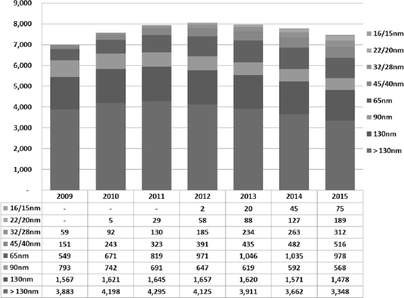
As a direct result of this trend the risk per design increases dramatically and more and more companies are already mandating prototyping of their designs prior to tape out to verify correctness and to avoid expensive re-spins. Prototyping can happen at various points in the design flow using a variety of different techniques. Overall, the decrease in design starts will only increase the risk per project even further and as a result prototyping will become even more important.
1.6.3. Increased programmability and software
The vast majority of electronic systems and products now include some element of programmability, which is in essence deferred functionality, which comes in several forms. First of all, estimates of the relative number of design starts for ASIC, ASPP and FPGAs show that the overwhelming number of design starts are in FPGAs and other Programmable Logic Devices; this clearly counts a programmable hardware.
Second, the number of FPGA design starts that include microprocessor units is growing very fast as well. This adds software programmability to programmable hardware.
In addition, a fair percentage of the ASIC and ASSP design starts contain embedded processors as well. As a result, the software adds programmability even dedicated SoC chips. As a result software is gaining significantly in importance, even in SoC projects.
Figure 8: Software effort as percentage of R&D expense (Source: IBS)
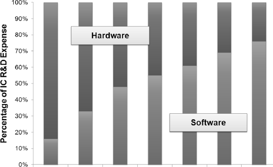
Figure 8 illustrates the projected software effort as percentage of R&D expense over technology nodes. At 65nm the expected R&D expense for software has surpassed that of hardware development.
Overall, software has become the critical path for chip development and its effort is surpassing that of hardware. In traditional serial design flows software development starts late, i.e., when hardware is well underway or even after final prototype chips are available. As a result software availability can hold up chip developments from reaching mainstream production.
From a prototyping perspective this represents yet another driver towards starting prototyping for software development as early as possible during a project. With software largely determining the functionality of a design, it is destined to also change verification flows. Software verification on prototypes will further gain in importance, as well as software becoming a driver for hardware verification too. As an alternative to classical verification using test benches coded in VHDL or SystemVerilog, directed tests using software have recently found more adoption.
Incidentally, this allows a new form of verification reuse across various phases of the development as described earlier.
To support this type of verification reuse, prototyping of the hardware as early as possible becomes mandatory. Given the seamless reuse of verification across various stages of the development, interfaces between different prototyping techniques have become more critical too. Virtual prototypes today can be connected to hardware-based prototypes to allow a mix of hardware- and software-based execution, offering a variety of advantages:
- First, avoiding having to re-model parts of the design which are already available in RTL reduces the development effort and enables hardware-assisted virtual platforms.
- Second, hardware prototypes can be brought up faster, because test benches – which traditionally can contain 50% of the overall defects – are already verified and stable as they have been applied to virtual prototypes before.
- Third, with a mix of hardware- and software-based techniques, trade-offs between accuracy, speed and time of availability of prototypes can be managed more flexibly.
- Finally, validation of the hardware/software prototype within the system context requires interfaces to the environment of the chip under development. Interfaces from hardware prototypes can execute close to, or even at, real-time. Interfaces using virtual prototypes can be made available even prior to actual hardware availability. For instance, USB 3.0 drivers were already developed on transaction-level models in virtual platforms, even before the actual cables were available.
1.6.4. Intellectual property block reuse
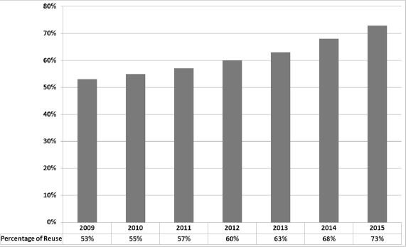
Another important trend is the reuse of IP blocks. With growing chip complexity, IP reuse has become an essential way to maintain growth of design productivity. Figure 9 shows that the percentage of reuse continues to increase and although not shown on this graph, since 2007 the reuse of blocks has increased from 45% to 55% i.e., most blocks are now reused in other designs.
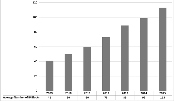
At the same time until the average number of IP blocks per chip has grown from 28 to 50, as shown in Figure 10. Both of these data points come from a study by Semico Research Corporation. Taking these IP trends into consideration, chip design itself is becoming a task of assembling existing blocks via interconnect fabrics. Chip differentiation can be achieved with custom blocks, custom coprocessors and, of course, with software.
There are various effects of increased IP reuse on prototyping. First, pre-defined IP models are pre-mapped and pre-verified in FPGA prototypes to decrease bring-up time and reduce unnecessary duplication of work. Users of IP also increasingly
Figure 9: Percentage of reuse of IP blocks (Source: Semico Research Corp.)
request model libraries at different stages of the project and at different levels of abstraction as part of the IP delivery itself. This is already very common in the area of processors, for which IP providers like ARM®, MIPS®, ARC® and Tensilica® are asked by their users to provide processor models which can be used for early software development and verification.
Figure 10: IP instances in SoC designs (Source: Semico Research Corp.)
While in the past, development of those models was a challenge because they had to interface to various proprietary simulation environments, the development of such models has recently become commercially feasible.
With the advent of standards like OSCI SystemC TLM-2.0, the models for processors, peripherals and interconnect have become interoperable across different SystemC-compliant simulation engines. Standardization implies the transition from an early adopter phase to mainstream, and as such availability of IP models has greatly improved.
1.6.5. Application specificity and mixed-signal design
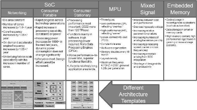
The target application markets for which chips are developed have a profound impact on the chip development itself. Figure 11 summarizes some of the defining characteristics of different target applications, according to the International Technology Roadmap for Semiconductors (ITRS).
ITRS differentiates between four major categories of chip design – SoCs, microprocessor units (MPUs), mixed-signal design and embedded memory. Each of the categories has specific requirements. To keep the die area constant while increasing performance is important for MPUs. Decreasing supply voltages are a key issue for mixed signal. Within the SoC domain the ITRS separates networking applications from consumer portable and consumer stationary, with various sub-requirements as shown in Figure 11.
Figure 11: Application specific requirements (Source: ITRS)
Overall, the end application has become more important for chip design requirements across the board and for SoCs specifically. As a result, prototyping in the different application domains requires application-specific analysis as well as application specific system interfaces, most of which have significant mixed signal content.
Besides other characteristics, the speed of external interfaces determines whether a prototype can be used directly or will need to be slowed down.
1.6.6. Multicore architectures and low power
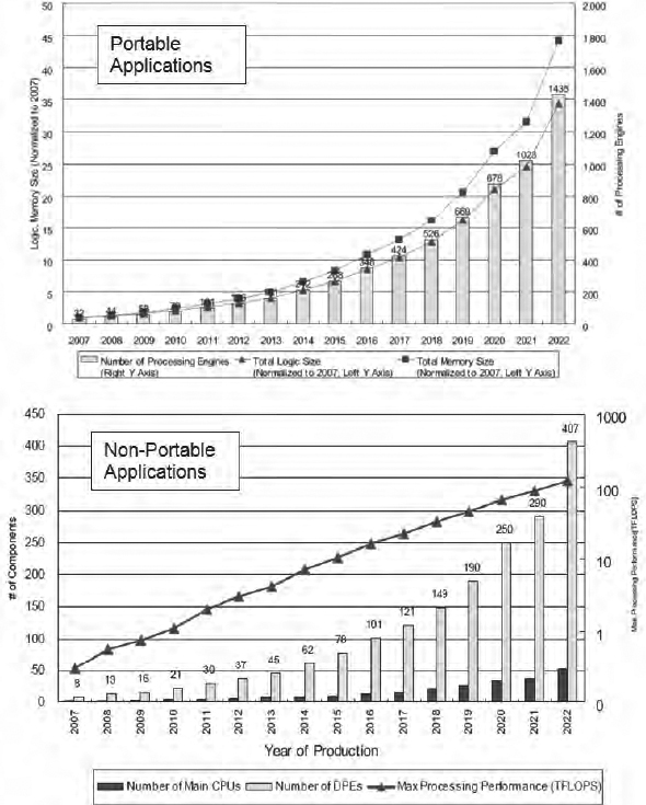
While for decades, the scaling of processors in speed has served the ever-increasing appetite of software applications for performance, the industry has run into limits around 4GHz for CPUs and 1GHz for embedded processors. The reason for that limitation lies in power consumption, which simply exceeds power envelopes when just scaled higher. This real and hard limitation has led to a trend to switch to multicore architectures. Simply put, more cores at lower frequency will result in less power consumption than simply scaling one core. The graphs in Figure 12 confirm this trend in CPU and data processing engines (DPE) usage for consumer applications, portable and non-portable.
We can see that the average number of DPEs, for example, has almost tripled from 2007 to 2011 and is expected to increase further. While this is a good solution on the hardware side, the challenge has now been transferred to the software side.
Traditionally, sequential software now needs to be distributed across multiple cores. For prototyping this means that debugging (the ability to look into the hardware/software execution) has become more important as well as the ability to start, pause, resume and stop hardware/software execution.
Today’s virtual prototypes already offer intelligent techniques to un-intrusively debug design and they can be started and stopped at any given time. Demands on debug and control for hardware-based prototypes have also increased, but debug capabilities in FPGA-based prototypes still trail those of virtual prototypes.
Figure 12: CPU requirements for consumer applications (source: ITRS)
1.7. Summary
Prototyping, in all its forms, provides powerful methods for verifying the design of hardware and validating the software in models, which to a greater or lesser degree, mimic the target environment. FPGA-based prototyping is especially beneficial during the crucial later stages of the project when hardware and software are integrated for the first time. Users have several prototyping options and depending on their main requirements can choose between various software- and hardware-based techniques to prototype their designs.
Owing to the fact that design verification and software development now dominate SoC development effort, the use of prototyping has never been more important in reducing project duration and design costs. The various IC trends mentioned above lead us also to only one conclusion: prototyping has become a necessary element of chip design and will become only more crucial in the future, as we shall see in the final chapter of this book.
Figure 13: Users recognizing a variety of prototyping options
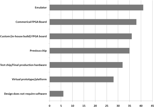
In this chapter, we have introduced a lot of terminology and some quite different types of prototyping. How widespread are each of them in real life? To answer this we refer to Figure 14 which summarizes 116 responses to a usage survey made during the SoC Virtual Conference in August 2009. When asked the question “What method(s) do/will you use to develop hardware dependent software (e.g., drivers, firmware) for your design project?”, the results show that users do indeed recognize a variety of distinct prototyping solutions. The results indicate that all the prototyping techniques described earlier are in active use – a clear result of the different priorities as discussed above – favoring different prototyping options.
In the following chapter we will zoom in on the benefits of FPGA-based prototyping in particular to software teams and to the whole SoC project.
The authors gratefully acknowledge significant contribution to this chapter from
Frank Schirrmeister of Synopsys, Mountain View