CHAPTER 4 |
GETTING STARTED |
So far we have explored the basic technology of FPGA devices and tools. For a first-time user of FPGA-based prototyping, it may seem a long leap to get from the fine-grain details of the target technology, to understanding how it may be employed to build a prototype. Later chapters will give all the necessary low-level technical details but first, it may be useful to answer the question “where do I start?” This chapter is intended to do precisely that. We will first look at the steps required and help the reader to ascertain the necessary resources, time and tooling required to get from first steps to a completed prototype project. At the end of this chapter, the reader should be able to know whether or not FPGA-based prototyping of an SoC design can be successful.
4.1. A getting-started checklist
To set the scene, Table 7 has a framework of the main tasks and considerations during the project, broken into two main phases; set-up phase and the usage phase.
It may be obvious that most of the effort comes during the set-up phase but most of the benefit is reaped during the use phase.
The steps in the checklist follow the same order as the chapters and subjects in this book and both reflect the decision tree through which the reader should already be traversing. In FPGA-based prototyping, the SoC design is mapped into a single or multiple FPGAs, emulating the SoC behavior at, or close to, the intended SoC speed. Each subject area will be explored in detail later, but first, let us look more closely at the tool and process flow at the heart of an FPGA-based prototyping project.
Table 7: A getting-started checklist
| Phase | Tasks | Considerations |
| Set-Up | Choose FPGAs | How much capacity, speed, IO? |
| Build boards or buy boards | What expertise exists in-house? How much time is there? Does total cost fit in the budget? | |
| Get the design into FPGA | The “three laws of prototyping” How to minimize design changes How to track builds and revisions | |
| Usage | Bring-up prototype and find bugs | What instrumentation do we need? Can prototypes be shared? Is remote debug or configuration needed? |
| Run software | Will the software team use it standalone? How to link with software debugger? |
|
| Run in real world | How to ensure portability and robustness? Any special encasement needs? |
4.2. Estimating the required resources: FPGAs
The authors have seen situations in the past where novice prototypers have badly underestimated the FPGA resources required to map their designs. As a result, the platform, which had been designed and built in house, had to be scrapped, resulting in many weeks of delay in the project. This is an extreme example, but even if we do not overflow our available resources, we do not want to find ourselves in a situation where the FPGAs are too full, resulting in longer runtimes and lower performance.
At the start of the project, we need to establish what resources we need to implement the design and then allow for overhead. It is nevertheless important to establish an early and relatively accurate estimate for the required FPGA and other resources that we shall need. First, however, we need to decide how much of the SoC design will be prototyped and for this, we need to have early access to the SoC design itself. But how mature does the SoC design need to be in order to be useful?
4.2.1. How mature does the SoC design need to be?
We would like to have our FPGA-based prototype ready as soon in the project as possible in order to maximize the benefit to our end users e.g., software team and IP verification people. However, it is quite possible to start our prototyping effort too early and be wasting our time tackling RTL code which is too immature or incomplete. It is not an efficient use of prototyping time, skill and equipment only to find obvious RTL errors which are more easily found using RTL simulation. So how do we decide when is the optimum time to start our prototype?
There are probably as many answers to that question as there are prototype teams in the world and each team may have developed a procedure which they believe best suits their needs. For example, the prototyping team lead by David Stoller at TI in Dallas, USA, requires that the project RTL is complete and passing tests at a coverage of 80% or more before the RTL will be placed into a prototype. There are others who advocate that preliminary deliveries of RTL are usable when the code is only 75% complete. Whatever metric is used, in each case it is recommended that the release of RTL for prototyping is built into the overall SoC verification plan, like any other milestone.
All SoC teams will hold a plan for verification of all aspects of the design at various stages of the project. The aim of the plan is always 100% verification of the SoC and self-confirmation that this has been achieved. Some verification teams follow sophisticated methodology, such as the UVM (universal verification methodology), which is primarily intended for use with complex test-environments written in System Verilog. A verification plan records where verification engineers have decided to make certain tests and also the current state of the design with respect to each test. It will include various milestones for the maturity of the project and especially its RTL. For good integration of FPGA-based prototyping into the whole SoC project, the verification plan should also include milestones for the prototype itself. Basic milestones might be when RTL is ready for check-out, when the FPGA-ready RTL has passed the original test bench or when basic register access on the board is running etc. Integration of FPGA-based prototyping into verification plans is part of Design-for-Prototyping, which is covered in chapter 9.
To come back to our question of when the RTL is ready for prototyping, a good general guide is to sync the first delivery of RTL with the point in the SoC project where trial implementation of the ASIC flow is started. This is typically where the RTL has been tested at each block level and has been assembled enough to run some basic, early tests. Some teams call this the “hello world” test i.e., the RTL is assembled into a simulator and a test bench is able to run vectors in order to load and read certain registers, see ports and pass data around the SoC etc. If the design is passing such tests in the simulator then it should also be at least able to pass this in the prototype, which is a good indication that the prototype is ready to make its contribution to the validation effort. For more information about use of “hello world” tests and prototype bring-up, see chapter 11.
4.2.2. How much of the design should be included?
Early in the prototyping effort, we need to establish the scope of the prototyping. The considerations are usually a mix of the architecture and scale of the design to be prototyped, and the available prototyping options. Before we consider the partitioning between multiple FPGAs we need to apportion which parts of the SoC design will be placed into FPGA and which may be better placed elsewhere, or even left out altogether.
Figure 44: Coarse partition of design into FPGA or external devices.
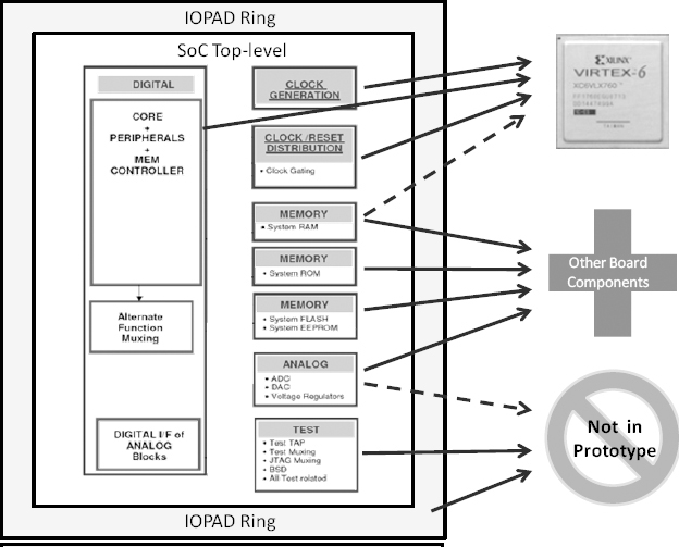
Figure 44 shows an overview of the top level of a typical SoC. Most of the SoC digital blocks can be placed inside FPGA resources but other blocks will be better placed in external resources, particularly memories. The analog sections of the SoC might be modeled on-board but some may choose to leave the analog out and prototype only the digital portion. The IO Pad ring is normally left out from the prototype along with the test circuitry as the prototype is focused upon functional test of the digital RTL and creating a working model for the software, which does not typically interface with the test system.
When evaluating the design intended for prototyping, the design can generally divided into two categories: what can go into FPGA, and what cannot go into FPGA.
4.2.3. Design blocks that map outside of the FPGA
While FPGA is the main prototyping resource in a typical prototyping system, typical SoCs are likely to have blocks that either do not map into FPGA, or blocks for which better prototyping resources are available. Such blocks are typically either analog circuits or fixed digital IP blocks for which neither source code nor FPGA netlist is available. In either case, we need to consider resources other than FPGA to prototype them.
For evaluation purposes, IP suppliers typically provide evaluation boards with the IP implemented in fixed silicon. In other cases, the prototyping team may design and build boards that are functionally equivalent to the IP blocks that do not map into FPGA. In yet other cases, existing or legacy SoCs may be available on boards as part of the prototyping project and can be added to and augment the FPGA platform. The advantage of using such hard IP resources is their higher performance as compared to FPGA implementation and their minor FPGA footprint.
To accommodate for the inclusion of these external hardware options, we need to verify/perform the following:
- Electrical connectivity: provide connectivity in the RTL to modules that are external to the FPGA.
- Signaling: make sure the IO signaling levels between FPGA and external hardware modules are compatible with each other. Also, make sure the signal integrity of the external hardware is acceptable to both FPGA and hardware module. Typical FPGA IOs have a number of options such as signaling levels, edge speed and drive strengths. We should be familiar with these options and how to best use them in the particular prototyping environment.
- Clocking and timing: provide the needed clocking, account for the clock delays and calculate the interconnect timing between FPGA system and external hardware.
- Logic synchronization: cold start-up time of fixed hardware is likely to be much shorter than that of the FPGA system as the FPGAs need to be loaded before they become functional. Early start can result in synchronization problems between the hardware modules and the FPGA system. We need to understand these issues and account for synchronous and asynchronous resets, and pulse durations for all cold and warm restarting conditions.
- Physical/mechanical: plan how the external blocks will physically connect to the FPGA system and how power is supplied. Care must be paid to cabling and repeated connection to the FPGA system to protect both the FPGA and the hardware module. A good mechanical plan will make it easier when the prototyping needs to be shipped to a remote lab or a customer.
Clearly only design elements that can map into FPGA may be included so, for example, analog elements will need to be handled separately. When evaluating the scale of prototyping there are some trade-offs that must be considered. Specifically, design size, clock rates and design processing times are inter-related and will mutually affect each other. While there are examples to the contrary, for a given platform, smaller designs generally run at faster clock rates and take less time to process than larger designs. We should therefore be wary of including more of the SoC design into the prototype than is useful. In which ways can we reduce the scale of the prototype without overly reducing its usefulness or accuracy?
To reduce the size of the design and to ease the capacity limitat ions, the following options can be considered:
- Permanent logic removal: when blocks in the SoC design have a hardware equivalent (physical SoC, evaluation platform etc.) that can be added to the FPGA platform, then it is a good candidate for removal from the logic that will map into the FPGA. In addition to space relief, these blocks can run at faster speeds than the attainable speed in the FPGA platform. Typical examples for such blocks are third-party IPs such as a processor, or special purpose controller.
- Temporary logic removal: when the amount of logic exceeds the feasible space in the FPGA platform, temporary removal of some blocks may be considered. This can work when parts of the SoC can be prototyped at the time. For example, if an SoC has multiple possible memory interfaces but only one will be used in the actual application, then prototyping them one at a time, while the others are removed, will verify each one in isolation of the other.
- Block scaling: when the size of blocks in the SoC will exceed the available feasible space in the whole FPGA platform, scaling them down may be considered. For example, SoC memory block may be scaled down to run subsets of the code at any given time, or alternatively, one channel of a multichannel design might be sufficient to represent enough functionality for the purposes of prototyping the channel-driver software.
Each of these recommendations is discussed in greater detail in chapter 7
Once the portion of the design to be prototyped has been selected, it is important to estimate up-front how well the remaining design will fit into FPGA technology. To do this estimation, it is obviously important to understand the FPGA’s resources available in our prototype platform. A too-simple early estimate that such-and-such FPGA contains n million gates will often lead to difficulties later in the project when it appears that the design is taking more FPGA resources than expected.
4.2.4. How big is an FPGA?
As covered in detail in chapter 3, an FPGA is an excellent resource for prototyping. Not only does it contain copious amounts of combinatorial and sequential logic but it also contains additional resources such as various types of memory and arithmetic blocks, and special IO and interconnect elements that further increase the scope of FPGA technology for prototyping.
The heterogeneous nature of modern FPGAs makes the answer to the question “how big is an FPGA?” rather difficult. The generic answer might be “it depends.” We will give some idea of the raw capacity of various parts of an FPGA below, but in fact, their use in an FPGA-based prototype will depend on the requirements of the design, the power of the tools employed and the amount of effort put in by the prototyping team. Let us consider the raw capacity of different resources in an FPGA. We use a Xilinx® 6VLX760 (or just LX760 for short) as an example and will provide a capacity figure for each resource in SoC gates.
- Logic: FPGA implements logic in highly configurable cells combining look-up tables with optional output FFs, carry logic and other special elements for efficiently mapping logic.
- The LX760 has approximately 750,000 look-up tables and 950,000 FFs. This is sufficient to map approximately four million SoC logic gates if fully utilized, or approximately 2.5 million gates at reasonable utilization.
- Memory : in addition to the look-up tables, which can be configured as small memories, dedicated memory blocks are also distributed throughout the device, which can be used as single- or dual-ported R/W synchronous memory blocks. These memory blocks can be connected together and form deeper or wider memory blocks and with addit ional built-in logic can be used to implement specialized memories such as single- or dual-clock FIFOs. These are often configured from a library of specialist memory IP available from the vendor.
- The LX760 has 720 memory blocks which can provide approximately 26Mbits of memory in various configurations (ROM, RAM, FIFO). In addition if logic cells are used as memory then a maximum 8.3Mbits of extra memory is available, but this would reduce the amount of logic available accordingly.
- DSP resources: it is also common for the latest FPGAs to have dedicated DSP blocks distributed throughout the device, which include MAC (multiply/accumulate) blocks, barrel shifting, magnitude comparators and pattern detection. In addition, DSP blocks have cascading capabilities that allow them to be connected together to form wider math functions such as DSP filters without the use of logic FPGA resources.
- The LX760 has 864 DSP blocks. These are very dense blocks and many hundreds of equivalent gates of logic can be implemented in each one. For those designs which have significant arithmetic content, good use of DSP blocks will liberate many thousands of logic elements for other purposes.
- IO: FPGAs’ IOs can be configured in many ways to comply with a variety of standards, drive strengths, differential pairs, dynamically controlled impedances etc.
- The LX760 has 1200 usable IO pins which can be combined to produce up to 600 differential pairs. Signaling between FPGAs is often a more critical resource than the logic or memory capacity.
- Interconnect resources: possibly the most important resource in an FPGA is the means to interconnect between the various blocks. With the exception of some special buffers, these resources are generally not explicitly controllable by the user but rather, they are used implicitly by place & route and some advanced physical synthesis tools in order to implement a design’s connectivity on the FPGA.
- Clocking resources: a subset of the interconnect is dedicated to implementing the design’s clock. These are dedicated programmable clock generators including PLLs, and global and regional clock buffers and low-skew distribution networks.
- The LX760 has 18 very sophisticated multi-mode clock managers (MMCM) blocks providing global or regional low-skew clocks.
- Special purpose blocks: finally, some devices have hard-macro blocks which implement specific functions such as Ethernet MACs, PCI Express interface blocks, selected CPU cores or high-speed serial transceivers (e.g., SERDES). These macros help implement industry standard peripheral interfaces such as PCI Express or Ethernet.
Recommendation: given the dedicated nature of the special-purpose resources, SoC logic will probably not map transparently into these resources. In order to use the special purpose resource, some SoC design blocks may need to be swapped with FPGA equivalents. When such design changes are made, it should be understood that the functional behavior of the new block may not be identical to the original.
For more FPGA resources details refer back to chapter 3.
For more information on replacing SoC design blocks with equivalent (or near equivalent) FPGA cores see chapter 10 on handling IP.
4.2.5. How big is the whole SoC design in FPGA terms?
This estimate may be critical to the scale of system to be used. The largest of FPGA currently available at time of writing this manual is the Virtex®-6 LX760 from Xilinx. As we have noted above, this device has a variable mix of over 4 million SoC-equivalent logic gates, approximately 25Mbits of memory, and over 850 48-bit multiply/accumulate blocks. As we write this, that resource list seems impressive but if the history of FPGA has taught us anything it is that the FPGA which invokes awe today will be commonplace tomorrow. Therefore if this manual is being read some years after its initial publication, please scale up the figures to whichever behemoth FPGA is under consideration.
How will the FPGA’s impressive resource list be able to handle the SoC design? The answer, of course, is that it is design-dependent. Given the “flip-flop rich” FPGA architecture, highly pipelined designs with a high ratio of FFs to combinatorial logic will map better into FPGA than designs with lower ratios. It will also most likely run at a faster clock rate. We do not always have the luxury of receiving an SoC design which is conveniently FPGA-shaped and so there are a number of steps which are usually required in order to make the design FPGA-ready. These are detailed in chapter 7.
The mix of the different resources varies device to device, as some devices have more of one type of resources at the expense of others. A casual use of gate-count metrics may lead to misunderstanding and the safest way to estimate the necessary FPGA resources for the design is to use FPGA synthesis upon the design to gain an estimate of total FFs, logic cells and memories. This requires the RTL to be available, of course, and also usable by the FPGA synthesis tool of choice.
It’s important to note that in terms of gate-count metrics, FPGA technology and SoC technology do not compare well, and FPGA gate counts are given as a rough approximation.
Even if all SoC logic may be mapped into FPGA, the utilization may be limited owing to one or more of the following reasons:
- The design: some designs map more effectively into FPGA resources than other designs due to how well they fit FPGA architecture and resources. As described above, since FPGA technology is flip-flop rich, designs with a higher FF to combinatorial logic ratio are likely to achieve higher effective gate count levels than designs having a lower ratio.
- Clock resources: while having multiple clock regions/zones, FPGAs have a finite resource of PLL, clock multiplexers and on-chip clock routes (refer back to chapter 3). A closer look at the available clocking resources and clock zones restrictions in the selected FPGA is necessary for multi-clock designs.
- FPGA routing resources: FPGA’s useable logic may be limited by the availability of routing resources which may vary from design to design. “Highly connected” designs may exhaust FPGA routing resources in some areas and restrict access to FPGA resources in that area, possibly rendering them unusable. In addition, such designs are likely to run at reduced clock rates as compared to “lightly-congested” designs.
- FPGA IO pins: it is very common with modern SoC designs for the FPGAs in a multi-FPGA partitioned design to run out of pins before they run out of logic or memory. Intelligent partitioning, which balances resources between FPGAs, may still need to use multiplexing to route all signals between the FPGAs (see chapter 8).
Recommendation: FPGA designs with high utilization levels are less likely to run at the peak clock rates. Also, highly utilized designs run the risk of exceeding available resources if or when the design grows because of mid-project design changes. While FPGA utilization levels of over 90% are possible, it is recommended to limit initial utilization levels to 50%.
4.2.6. FPGA resource estimation
In estimating the FPGA resources used in a given SoC design, the resources that need estimation are: FPGA IO, random logic, FFs, memory blocks, arithmetic elements and clocks. Manually estimating resources such as memory blocks, multipliers and high-speed IO is fairly straight forward and fairly accurate but estimating random logic and FFs is more difficult and the margin for error is greater. Therefore it is advised to first establish if the design will fit in an FPGA based on the special resources and as soon as the design is synthesizable run it through the synthesis tool for an accurate FPGA resources usage estimate. If the design is synthesizable, it is recommended to use a quick synthesis evaluation that will indicate expected resource utilization.
Once the FPGA resources utilization levels for a given design are available, we need to establish the utilization level target for the maturity level of design. As a general rule, the higher the FPGA utilization level the longer it will take to process the design (synthesis, place & route etc.) and the slower the system clock will run due to greater routing delays. In addition, during the prototyping project the design is likely to change and some diagnostics logic may be added in the future, so the number of FPGAs in the system should be considered conservatively.
On the other hand, distributing the design to many FPGAs adds cost and implementation complexity. While design size and performance can vary from design to design, it’s recommended the utilization levels should initially be below 50%. Even lower utilization is recommended for partial designs that are expected to grow. It is always recommended to overestimate resources because project delays caused by underestimation can be more costly than the price of unused FPGA devices purchased based on overestimation.
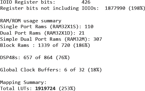
The synthesis tool will then provide a resource list for the design as a whole, for example, Synplify® Premier FPGA synthesis tools provide a list such as the one shown in Figure 45 . We see the results for a large design mapping “into” a single Xilinx® 6VLX760 and even though the report may show that the resource utilization is far in excess of 100%, this is not important. Synplify Premier’s Fast Synthesis mode is particularly useful for this first-pass resource estimation.
Figure 45: Resource usage report from first-pass FPGA synthesis
In addition, some thought should be given to how much of the FPGA resources it is reasonable to use. Can the devices be filled to the brim, or should some headroom be allowed for late design changes or for extra debug instrumentation? Remembering that a key aim of FPGA-based prototyping is to reduce risk in the SoC project as a whole, it follows that squeezing the last ounce of logic into the FPGAs may not be the lowest risk approach. In addition to leaving no margin for expansion, it is also true that FPGA place & route results degrade and runtimes increase greatly when devices are too full. A guideline might be to keep to less than the 75% utilization, which is typical for production FPGA designs and for prototyping projects, 60% or even 50% being not unreasonable. This will make design iteration times shorter and make it easier to meet target performance.
From the results in Figure 45 we can see that the limiting resources are the LUTs (Look-up-Tables). For this design to fit into Virtex-6 technology on our prototyping board with 50% utilization, we will need a number of FPGAs calculated as follows:
Total LUTs required / LUTs in one device x 50%
= 1919724 / 758784 × 0.5
= approximately five 6VLX760 FPGAs.
Therefore, our approximation tells us that our project will need five FPGAs.
4.2.6.1. Size estimates for some familiar SoC blocks
It may help to get a feel for the resource in an FPGA by considering the sizes given, in FPGA terms, for some familiar blocks in Table 8.
Table 8: FPGA resources taken by familiar SoC functions
| IP / SoC function | FPGA resources required |
| ARM Cortex®-A5 (small configuration) | Two Virtex-5 LX330 at 50% |
| ARM Cortex®-A9 | One Virtex-5 LX330 at 80% |
| ARM Mali™-400 w/3 pixel processors | Four Virtex-5 LX330 at 50% |
| ARC AS221 (audio processor) | One Virtex-5 LX330 at 10% |
| ARC AV 417V (video processor) | One Virtex-5 LX330 at 60% |
These are only rules of thumb as each of these IP or processor examples have a number of configurations, memory sizes and so forth. However, we can see that even as FPGAs continue to get bigger, the first law of prototyping still holds true.
Recommendation: To manually estimate the required FPGA resources can be difficult, time consuming and may be quite inaccurate. It’s often more effective to run preliminary synthesis and quickly find out the FPGA resource usage levels and have initial performance estimation.
4.2.7. How fast will the prototype run?
Performance estimation is tightly coupled to the resource utilization levels and the FPGA performance parameters. Similar to FPGA resource estimation, performance estimation for the special blocks is easily extracted from the timing information in FPGA datasheets. Estimating the overall performance is much harder. However, a fairly good performance estimation of the whole design is easy to obtain from the synthesis tool. Although the synthesis tool takes in account routing delays, the actual timing depends on the FPGA place & route process and it may differ from the synthesis tool’s estimation. While the difference can be significant with higher utilization levels as routing can become more difficult, the initial timing estimation is quite a useful guide.
FPGA performance greatly depends on the constraints provided to the synthesis tool. These constraints direct the synthesis tool and subsequently the place & route tools how to best accomplish the desired performance. For more details on how constraints affect the FPGA implementation, refer to chapter 7.
There are a number of factors affecting the clock rate of a design mapped into a multi-FPGA system, as described below:
- Design type: highly pipelined designs that map well into FPGA architecture and leverage their abundant FFs are likely to run faster than designs that that are less pipelined.
- Design internal connectivity: designs with complex connectivity, where many nodes have high fan-out, will run slower than designs with lower fan-out connectivity due to the likely longer routing delays. It will also be harder to find places in the design where a partitioning solution is possible with few enough IO to fit within an FPGA footprint. Higher interconnected designs will more likely require multiplexing of multiple signals onto the same IO pins.
- Resource utilization levels: typically the higher the utilization levels, the more congested the design, resulting in longer internal delays and a slower clock rate. Below, we explore the recommendations for device utilization.
- FPGA performance: the raw performance of the FPGA itself. Even with the most tailored and optimized design, we will eventually hit an upper limit for the FPGA fabric. In most cases, however, the non-optimized nature of the design and the efficiency of the tool flow will be seen as a limit long before the absolute internal clock rates of the FPGA.
- Inter-FPGA timing: in a multi-FPGA system, FPGA-to-FPGA clock skews and connectivity delays can limit the system clock rate. While FPGAs can theoretically run internal logic at clock rates of hundreds of megahertz, their standard IO speed is significantly slower and is often the prevailing factor limiting the system clock rates.
- External interfaces: as we shall explain later, SoC designs mapped into prototyping systems are likely to run at a slower clock rate than the SoC’s target clock. Other than the expected performance penalty, this is not a big issue for a closed system running with no external stimuli, or a system for which the stimuli can run at a slower rate to match the system’s clock rate. There may well be situations where the prototyping system must interface with stimuli that cannot be slowed down.
- Inter-FPGA connectivity: when all inter-FPGA connectivity is exhausted, pin multiplexing can be used. In time-domain multiplexing a number of signals share a single pin by running at a faster clock than the data rate of the individual signals multiplexed together. For example, when multiplexing four signals each running at the rate of 20MHz the combined signal will need to run at least at the rate of 80MHz and actually more, in order to allow for timing for first and last signals sampled. Since FPGA-to-FPGA data rate is limited by the physical FPGA pins and the board propagation delays, the effective data rate of the individual signals in this example will only be less than a quarter of the maximum inter-FPGA data rate.
Recommendation: pin multiplexing can severely limit systems’ clock, so it’s critical to evaluate the effect of partitioning on inter-FPGA connectivity during the early feasibility stage of the prototyping project. More detail on pin multiplexing is given in chapter 8.
4.3. How many FPGAs can be used in one prototype?
When designs are too large to fit into a single FPGA and still remain within recommended utilization levels, we must partition the SoC design over multiple FPGAs. While there is no theoretical limit to the number of FPGAs in a system – and so me designs will map well into large multiple FPGA systems – the eventual limit on the number of FPGAs in a prototyping system will depend upon both the design itself and the limitations of the prototyping platform.
In general, the following points will limit the number of FPGAs in a system:
- FPGA-to-FPGA connectivity: as designs are split into more FPGAs, inter-FPGA connectivity typically grows, and depending on the design and how it’s partitioned, it may exceed the available connectivity in a given system. Inter-FPGA connectivity is bounded by the available inter-FPGA connectivity in a given system. Depending on the systems, the inter-FPGA connectivity may be either fixed or programmable to some extent. A common technique to overcome inter-FPGA connectivity bottlenecks is to use high-speed pin multiplexing schemes in which multiple signals “time- share” a single connection. The time-domain pin multiplexing, however, requires a high-speed clock which may limit the system clock rate due to the timing limitation of the physical connection between the FPGAs.
- Signal propagation: since propagation delays to and from an FPGA’s IO pads are typically longer than propagation delays within the FPGA, signal propagation among FPGAs is typically the timing critical path and directly affects the system clock rate. Excessive FPGA-to-FPGA delays on the board (including long signal-settling times) will reduce timing margins and may limit the system’s clock rate. Signal propagation issues are more significant with greater number of FPGAs in the system due to the physical implementation, especially when connecting multiple boards together where signals go through multiple connectors and connection media (cables, other boards) and ground returns and reference may become marginal.
- Clock distribution: proper clock distribution in a synchronous multi-FPGA system is critical to its proper operation. Specifically, the clocks driving signals out from one FPGA and the clocks used to clock-in signals from other FPGAs must have minimal skew between the FPGAs exchanging data as to not violate setup and hold times. As systems grow larger with more FPGAs, the physical clock distribution may become harder to implement with an acceptable skew especially in scalable systems where multiple boards are connected together.
- Manual design partitioning: as the number of FPGAs in a system grows, partitioning becomes increasingly more complex, and manual partitioning may be impractical altogether. This may prove especially difficult if the partitioning needs to be modified often as the design changes.
- Managing multiple FPGAs: while not a technical barrier, the more FPGAs there are in a system, the more cumbersome the overall process is requiring a greater management effort. Specifically, a number of FPGAs may need to be re-processed (synthesis, place & route) with each design iterat ion, and processing multiple FPGAs in parallel requires multiple tool licenses for the software tools, otherwise the process becomes serial, taking longer to complete. In addition, each FPGA needs to be managed in terms of pin assignments, timing constraints, implementation files, revision control etc., which adds to the overall project engineering administration overhead.
When considering large multi-FPGA systems, it’s important to evaluate how well they address the above issues, and how well they scale. When either making boards in-house or buying in ready-made systems, such as Synopsys’ HAPS® and CHIPit®, the same FPGAs may be used but it is the way that these can be combined and interconnected that may be the limiting factor as projects grow or new projects are considered. The next three chapters aim to cover the ways that platforms can be built and configured to meet the needs of the specific project and/or subsequent projects.
Recommendation: early discovery of the design’s mapping and implementation issues is critical to the effectiveness of the prototyping effort. Using a partitioning tool such as Synopsys’ Certify® can simplify and speed up the partitioning process.
4.4. Estimating required resources
The various implementation and debug tools were described in chapter 3 but as a recap, a number of software tools are needed to map and implement the SoC into FPGAs. All tools come with their respective design environment or GUI, but can also be invoked from a command line or a script so that the whole implementation sequence can then be more efficiently run without supervision, for example, overnight.
The time taken to run the design through the tools will vary according to a number of factors including complexity, size and performance targets as we shall see below but runtime will always benefit from using more capable workstations and multiple tools in parallel. Readers may have some experience of FPGA design from earlier years, where a PC running Microsoft Windows® would suffice for any project. Today, however, our EDA tools used for prototyping are almost exclusively run on Linux-based workstations with more than 16Gbytes of RAM available for each process. This is mostly driven by the size of designs and blocks being processed and in particular, FPGA place & route is generally run on the whole design in one pass. With today’s FPGA databases having some millions of instances, this becomes a large processing exercise for a serious workstation.
In addition, we can increase our productivity by running multiple copies of a tool in parallel, running on separate workstation processors. For example, the synthesis and place & route on the different FPGAs after partitioning could be run in parallel so that the total runtime of the implementation would be governed only by that FPGA with the longest runtime.
4.5. How long will it take to process the design?
As a general rule, the higher the utilization level the lower the achievable clock rate and the longer the FPGA processing time. As we saw in chapter 3, the implementation process consists of the front-end and the back-end. Between them they perform five main tasks of logic synthesis, logic mapping, block placement, interconnect routing, finally, generation of the FPGA bit-stream. These tasks are summarized in Table 9.
Depending upon the tool flow, these tasks will be performed by different tools, the proportion of the runtime for each step will vary. For example, the traditional backend dominated flow has most of these tasks performed by an FPGA vendor’s dedicated place & route tools, hence the runtime is mostly spent in the placement and routing phases.
Table 9: Front-end and Back-end tasks for each FPGA
| Task | Description | |
| Front-end | Logic synthesis | RTL to behavior/gates |
| Mapping | Gates to FPGA resources | |
| Back-end | Placement | Allocate specific resources |
| Routing | Connect resources | |
| Bitstream generation | Final FPGA “programming” |
However, it is also possible to employ physical synthesis for the FPGA in which the front-end also performs the majority of the placement task. Consequently, more of the overall runtime would be spent in the front end.
Table 10: Tool runtime as proportion of whole flow (typical average)
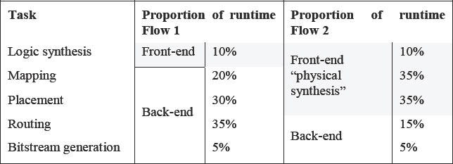
Table 10 shows the physical and non-physical flows side-by-side and gives the proportion of time typically spent in each step. These are only typical numbers of the relative time taken for each part of the process; real time will depend on the device utilization levels and timing requirements.
As we can see, placement and routing generally take longer than synthesis and as designs become larger and timing constraints more demanding, this becomes even more apparent. For example, a large FPGA at 90% utilization might easily take 24 hours or more to complete the whole flow; three quarters of that time being spent in place & route. When prototyping, this long runtime may be a large penalty to pay just to avoid using another, admittedly expensive, FPGA device. It may be better in the long run to use three FPGAs at 50% utilization, rather than two FPGAs at 75% each.
In general, FPGA physical synthesis is used for FPGA designs that are intended for mainstream production and require the best possible results. For FPGA-based prototyping, physical synthesis might be focused on one particular FPGA on the board which needs more help to reach the target performance.
Recommendation: FPGA designs with high utilization levels will take longer to process so while FPGA utilization levels of over 90% are possible, it is recommended to limit initial utilization levels to 50% in order to allow faster turnaround time on design iterations.
4.5.1. Really, how long will it take to process the design?
Avoiding answers that involve pieces of string, we should expect runtime in hours and not days. The aim should be a turn-around time such that we can make significant design changes and see the results running on the board within a day. Indeed, many prototyping teams settle into a routine of making changes during the day and starting a re-build script to run overnight and see new results the next morning. Automating such a script and building in traps and notifications will greatly help such an approach.
Long runtime is not fatal as long as we are careful and we get a good result at the end. Runtime becomes a problem when careless mistakes render our results useless, for example pin locations omitted or we iterate for only small changes.
If runtimes are too long to allow such a turn-around time, then we recommend taking some steps to reduce runtime. These might include some of the following:
- Add more workstations and licenses: this allows greater parallel processing and balancing of runtime tasks.
- Lower FPGA utilization: repartition design into more FPGAs. This may take some time but it may be an investment worth making. Total runtime can vary widely as a function of utilization level of the device.
- Note: It may be preferable to process six devices at 50% each rather than four devices at 75% each.
- Relax timing constraints: on less critical parts of the design it is possible to lower the timing goals to reduce tool runtime. Place & route runtime depends not only on utilization and other factors can have an even greater effect, including applied constraints, number of global clocks, and the number of clocks driving BlockRAMs. Basically, the more complex the task given to place & route, the longer the runtime.
- Use incremental flows: both synthesis and place & route have built-in incremental flows which reduce runtime by not re-processing parts of the design that are unchanged.
- Use quick-pass flows: some tools have options for turning off some optimization steps at the cost of lower quality of results. For example, the Fast Synthesis option in Synopsys FPGA synthesis tools.
- Relax timing model: in extreme cases, the timing model for the FPGA can be relaxed on the assumption that the device will not be used outside the lab and therefore temperature of voltage extremes built into the timing model will not apply.
Recommendation: To speed the implementation cycles, it is recommended to relax the timing constraints where possible as to minimize implementation times. Once the initial issues are resolved, and the implementation cycles are not as often, the more strict timing constraints can be applied.
4.5.2. A note on partitioning runtime
Somewhere along the way, it is probably going to be necessary to partition the design into multiple FPGAs. As we saw in chapter 3, partitioning could occur before logic synthesis i.e., by manually splitting the design into multiple FPGA projects, or after logic synthesis, by some database manipulation prior to mapping.
The runtime of partitioning tools is a relatively small part of the runtime for the whole flow and is not as greatly impacted by increased design capacity or constraint, as it is by the IO limitations. However, the automation of a partitioning flow may impact the success or otherwise of a scripted flow. We need a robust and tolerant methodology in the partitioning tool that can cope with changes in the design and, for example, not terminate when a new gate has appeared in the design because of a recent RTL change. The partitioner should be able to assume that if the new gate’s source and destination are in a given FPGA, then that gate itself should be automatically partitioned into that same FPGA. It would be rather frustrating to arrive at the lab in the morning after starting an overnight build script to discover a message on our screen asking where we want to put gate XYZ. So a partitioner’s runtime is less important than its automation and flexibility.
4.6. How much work will it be?
Implementation effort is divided here into the initial implementation effort, which are mostly performed only once in the prototyping project, and the subsequent implementation efforts which are repeated in each design iteration or “turn.”
4.6.1. Initial implementation effort
Initial activities for setting up the prototype mostly take place the first time the design is implemented where the infrastructure and implementation process are created and are then reused in subsequent design turns. The initial implementation efforts include the following:
- SoC design modifications: modifications done to the SoC design to better map it into FPGAs. This typically includes design optimization for performance (pipelining), trimming parts of the design not needed for prototyping, and replacing SoC structures with available FPGA structures, such as clocking circuits, memory structures etc.
- Partitioning: the process of dividing the SoC design into multiple FPGAs per the platform of choice.
- Design constraints generation: the process in which FPGA design implementation constraints are created. Typical constraints are pin placement, timing constraints and inserting synthesis directives.
- Debugging features: the process of configuring debugging features that will go into the design. This is an optional effort but is commonly used and typically repeated in subsequent design turns as needed.
- Physical design implementation: a series of processes necessary to implement the design. They include synthesis, mapping, place & route, timing analysis and bitmap generation. These activities are typically combined in implementation scripts that can be used in subsequent design turns.
The time it takes to accomplish the initial prototyping effort is usually the most significant in prototyping projects, especially for the first-time prototyper. This effort may involve learning new technologies and tools and acquiring platform and components, so overall effort may vary on a case-by-case basis. There is also the significant effort of adapting the SoC design for use in the FPGA, which is obviously design dependent.
Recommendation: To set expectations correctly, the initial implementation effort (excluding the platform and tool evaluation and training), for a four-FPGA system with each device resource utilization around 50% and a relaxed clock rate, might take ten to 16 engineer-weeks of effort, which is five to eight weeks for a typical two-engineer team.
4.6.2. Subsequent implementation effort
After the design has been successfully implemented once in the FPGA system and only small design modifications are needed, such as a result of bug discoveries, we will need to make design changes. Typically these will only have a small impact on partitioning and design constraining and therefore mostly involve the design implementation phase once the whole implementation process is set up. Assuming the design implementation is scripted into “build” or a “make” files, this effort is fairly small and is limited to implementing the design changes, running the implementation scripts and reviewing various report files.
Recommendation: where possible, use the incremental design features through the implementation chain to minimize implementation time for minor design changes.
The time for subsequent implementation depends on the extent of design modification compared to the previous run:
- Minor modifications: for minor changes, such as changing debug probes or small logic changes to the design itself, re-implementation of the design requires only synthesis, place & route. Implementation tools can be configured to operate in an incremental mode where only blocks that have changed require re-synthesis and place & route, which translate into significant processing time savings. For such cases implementation time can typically be one to four hours per FPGA.
- Moderate modifications: at this point the design may have grown beyond the initial 50% utilization levels target, and the timing requirements may be harder to accomplish. If the design changes are significant then implementation may involve partition changes. Therefore, such iteration may take as much as a couple of days.
4.6.3. A note on engineering resources
First-time prototypers should not make the mistake of thinking that making an FPGA-based prototype is a summer job for the intern. For a successful and productive prototyping project there needs to be a good understanding of the design to be prototyped, of the FPGA technology, of the tools necessary and prototyping optimization techniques. Since prototyping is often critical to the overall SoC project schedule, it is recommended to dedicate at least one engineer with a good RTL knowledge, a good understanding of FPGA technology and tools, and good hardware and at-the-bench debugging skills. These are not skills typically found in SoC verification teams and so some consideration of building and maintaining such expertise in-house should be undertaken.
Larger corporations with multiple prototyping projects typically retain a team of engineers specifically for FPGA-based prototyping tasks. Such a valuable expert resource has a high return-on-investment, as SoCs, and the software running on them, benefit from better verification.
In some cases it is possible to share some of the tasks among multiple engineers. For example, to identify multi-cycle paths to relax the timing constraints or to make RTL changes to improve timing, the SoC engineers may be a good choice to implement these tasks since they are most familiar with the design and can resolve these issues more effectively.
Recommendation: for a first-time prototyping project, it is recommended to make use of consultants who can provide the necessary front-to-back prototyping expertise. Employing and learning from such experts is a very productive way to get up to speed with prototyping in general while also benefiting the current project.
4.7. FPGA platform
After estimating the logic resources needed, the size of the system should become evident. Specifically, the type of FPGAs to use, the number of FPGAs needed, the interconnect requirements, and additional hardware such as external memories, controllers, analog circuitry etc., that will be added to the FPGA system. At this point in time, the decision whether to buy an off-the-shelf FPGA system or to develop it in-house must be made. Some of the important considerations are how well the system scales with design size changes and the potential reuse of the system for future prototyping projects, where the more “generic” the platform is, the more re-usable it will be in future projects.
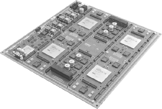
As an example of the types of ready-made FPGA platforms available, Figure 46 shows a platform from a Synopsys HAPS® (High-Performance ASIC Prototyping System) family of boards.
This example shows a HAPS board which has four Virtex-6 LX760 FPGAs, plus a smaller fifth FPGA, which is used to configure the board and also holds the supervisor and communications functions. There are other HAPS boards which have one or two LX760 devices each but with the same level of infrastructure as the board with four FPGAs. So we have the same resource in effect in three configurations i.e., single, double and quadruple FPGA modules which can operate independently or be combined into larger systems. The HAPS approach also includes different connectivity options and separate add-on boards for various hard IP, memory, and IO options.
Figure 46: Example of a ready-made FPGA platform, HAPS®-64
The importance of such flexibility becomes apparent when platforms are to be reused across multiple prototyping projects. The options and the trade-offs between making project-specific boards and obtaining third-party ready-made boards like HAPS are described in more detail in the “Which platform?” chapters (5 and 6) so we shall not cover in any more detail here.
4.8. Summary
We have now covered all the reasons why we might use FPGA-based prototyping and which types, device, tools and boards might be most applicable in given situations. We have decided which parts of the design would most suitable for prototyping and how we can get started on our project.
The most important point to be re-iterated from this chapter is that there is an effort ‘vs’ reward balance to be considered in every project. With enough time, effort and ingenuity, any SoC design can be made to work to some degree in an FPGA-based prototype. However, if we start with realistic and achievable expectations for device usage and speed, and omit those design elements which bring little benefit to the prototype but would take a great deal of effort (e.g., BIST) then we can increase the usefulness of the prototype to most end-users.