CHAPTER 5 |
WHICH PLATFORM? |
It is important to explore the different options for target FPGA platforms at an early stage. The most obvious choice from the start is whether to design and make your own specific boards or to obtain boards from an external supplier. The next two chapters will discuss technical aspects of the platform choice, starting with this chapter, in which we will focus on making your own boards in-house. There is also some detail in Appendix B on making an informed comparison from an economical and business perspective.
5.1. What is the best shape for the platform?
In earlier chapters we explored the many possible aims for an FPGA-based prototyping project; by the time we get to choose the platform, the basic needs for the project will probably be well understood. On the other hand, there may be a whole series of projects for which a platform is intended, requiring a more forward-looking and generic solution to multiple needs. The platform’s topology, that is, the physical and electrical arrangement of its resources will need to meet those needs.
Let us consider the topology needs as divided into the following areas:
- Size and form factor
- Modularity
- Interconnect
- Flexibility
each of which we will now give further consideration.
5.1.1. Size and form factor
Clearly, an FPGA-based prototype will take more space in the final product than that occupied by the intended SoC, but in most cases we are not looking for an exact physical replacement of one by the other. How close to final form-factor does the FPGA-based prototype need to be?
In many cases, umbilical cable may be used to connect the FPGA platform to the in-system socket of the intended SoC. In that case, electrical and timing considerations would need to be understood. For example, do the FPGA IO pins have the electrical characteristics required to drive the cable load as well as the final SoC load. Would the cable require high-drive buffers to make this possible? If so, we should also then account for the buffer delays as part of the IO constraints for the implementation tool flow.
The advantage of having an umbilical cable to a final SoC socket is that the platform may be more easily used as a demonstration model for external suppliers, partners or investors. If this is an important aim then it might also be worth considering the use of a complimentary virtual prototype for early demonstrations, potentially linking this to part of the FPGA platform in a combined hybrid prototype environment.
It is not common to find these umbilical topologies in real-life FPGA-based prototyping projects. In fact, a more widespread approach is almost the opposite with the SoC first sample silicon being more often plugged into a pre-prepared location on the FPGA-based prototype platform, rather than the other way round as discussed above. This requires a hardware topology in which there is a physical partition at the SoC pins; that is, between the contents of the SoC (i.e., pins-in) and the rest of the system (i.e., pins-out). That may seem natural and obvious but in-house boards can often mix everything together, especially when the boards are intended to be used only for a single project.
Figure 47: FPGA-based Prototyping platform employing a personality board
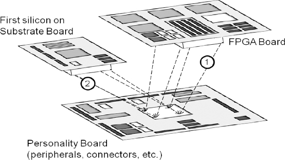
A diagram of this pins-in/pins-out hardware topology is shown in Figure 47. Here we see a personality board for the pins-out portion of the prototype, including peripherals which represent the interface for the SoC with its final target product. The personality board is connected via a header to the pins-in portion of the design which is modeled on an FPGA board. Upon receipt, the first silicon is mounted on a substrate board and fitted onto the header in place of the FPGA board.
User often tell us that when first-silicon is introduced into a previously working prototype platform in this way then software can be up and running in only a matter of hours. This is an excellent example of how some forethought regarding the topology of the FPGA-based prototyping platform can greatly improve productivity later in the project.
5.1.2. Modularity
The specific case of a pins-in/pins-out topology partition leads into a more general discussion of modularity. When building an FPGA-based Prototyping platform, should all components be placed onto one board to potentially increase FPGA-to-FPGA performance or should different types of component (e.g., FPGAs, peripherals, memories) be placed on separate boards, to potentially increase flexibility? Or is there perhaps some hybrid arrangement of the two? There is no one right way for all cases but in general, what starts as a question of flexibility versus performance, becomes more a matter of cost, yield and manufacture, as we shall discuss later.
Considering just the flexibility versus performance question for the moment, an arrangement of mother-board and daughter-boards may be a good compromise. If the boards are intended for multiple projects, it makes sense to group components into those which will always be required for every project and those which are only required occasionally. Ever-present components may then be placed on a motherboard along with the FPGAs and other global resources. Those components which are specific to a given project may then be added as daughter boards as required. For follow-on projects, the hardware re-design will then be limited to one or two daughter boards rather than an entire platform.
5.1.2.1. Mother and daughter cards vs. “all-on-board”
It is often tempting to make one large single board to fit the whole design and indeed, this can be good for a very targeted or application-specific solution, especially if it does not require a large number of FPGAs and has a well defined set of peripherals. For example, if we are always expecting to prototype video graphics designs, then we might always add an on-board VGA or other screen driver port. If we are in a networking design team, then an Ethernet/IP port would probably always be necessary.
Figure 48: Inefficient use of FPGA IO pins owing to dedicated peripherals
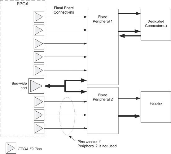
However, as a note of caution, peripherals on an FPGA motherboard are likely to be connected directly to FPGA pins, as shown in Figure 48.
If the peripheral is not used for a particular design, then the FPGA IO pins would still be connected to the unused peripheral and therefore not available for any other purpose, limiting the overall capacity of the motherboard. In addition, effort must be made to ensure that the unused peripheral remains dormant or at least does not interrupt the operation of the rest of the board.
The common solution to avoid this compromise is to place the peripheral on a separate daughter card so that it can be connected into the system when necessary and otherwise removed. If we have an attitude to on-board peripherals of “if in doubt, put it on” then we may severely limit the most valuable resource on the motherboard, i.e., the IO pins of the FPGAs themselves.
5.1.3. Interconnect
As mentioned, the FPGA IO pins and the connections between the FPGAs should be considered the most valuable resources on the platform. This is because they are the most likely to be 100% used, especially when a non-optimal partition is employed. What is the best Interconnect topology for a given design and partition (or for a given set of designs, assuming reuse is desirable)?
Given that in-house platforms will often be designed and built with a specific SoC project in mind, the connectivity between the FPGAs will tend to resemble the connectivity between major blocks at the top-level of the SoC design. This is especially likely if the SoC has been designed with the platform in mind. This may seem a circular argument but it is not. This is because many designs are derivative of previous versions and also because Design-for-Prototyping methods will tend to group the SoC’s top-level hierarchy into FPGA-sized blocks. With the platform interconnect being fixed and matching the SoC top-level connectivity the partitioning of the design becomes easier. The downside is that the reuse of the board for follow-on projects becomes harder, as will be seen in the next section.
For a platform to be more generic and therefore more likely to be re-usable across multiple projects, the interconnect resource should be as design-independent as possible, although perhaps constrained by some ever-present design elements such as the width and number of buses in the SoC or a particular data-path arrangement between the SoC and system-level elements. If projects are always standardized around a specific bus specification, for example, then inter-FPGA connection needs can be anticipated to some degree.
For example, if a 64-bit AHB™ bus is always employed then connectivity on the board can be provided to carry the bus between all FPGAs. It should always be remembered, of course, that an AHB bus and other standardized bus systems require many more pins than may be inferred by their nominal width. For example, a 64-bit bus might have 64 bits of address, 64 bits of write data, 64 bits of read data and 10 or 20 or more control and status signals, e.g., rd, ale, rdy etc. This would total over 200 or more connections at each FPGA that resides on the bus, which is a sizeable proportion of the total inter-FPGA IO connections available. Even if the address and data were multiplexed, the number of global pins and traces would be over 130.
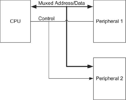
Consider the example in Figure 49, which shows a simple 64-bit multiplexed address-data bus connection between a CPU and two peripherals.
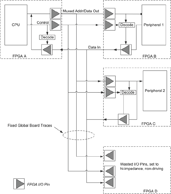
It is quite possible that a situation would arise where this circuit were mapped to three FPGAs as shown in Figure 49 with a fourth FPGA on the same board not required to house a bus peripheral, but instead some other part of the design.
Without care and foresight, wider buses and datapaths can run out of interconnections on a given board. It is necessary to fully understand the top-level topology and interconnections at the SoC top-level but it is also recommended to build flexibility into the board interconnect resources. This could be done using cables or switch matrices rather than using fixed traces in the PCB itself.
Figure 49 : Multiplexed address-data bus before partitioning (compare with Figure 50)
If the board has fixed global resources routing the bus to every FPGA then the fourth FPGA (FPGA D in the example shown in Figure 50) would not be able to use 130+ of its precious IO pins. These would need to be set to high-impedance, non-driving mode so as not to drive or excessively load the traces being used to route the bus between the remaining FPGAs. We shall revisit this example in chapter 6 when we consider commercially sourced boards and how the limitations of interconnect can become a very critical factor.
Figure 50: Multiplexed address-data bus from Figure 49 after partitioning
5.1.4. Flexibility
How flexible does the platform need to be? It may be decided from the start of the project that the platform will only ever be used for one prototype; follow-on reuse would be a bonus but is not necessary to justify the project or its budget. This simplifies matters considerably and is the most common compromise when designing in-house platforms. Indeed, in the authors’ experience, most in-house platforms are never reused for follow-on projects. Not only because that was never the intent (as above) but also because, even when intended for reuse, the boards themselves do not have the resource or interconnect to allow it. In those cases where in-house board development was only funded by management based on a multi-project return-on-investment, if this turns out not to be possible then we might jeopardize use of FPGA-based prototyping in future projects. We can see then that building in flexibility can be highly beneficial, despite the necessary extra complexity.
For maximum re-usability, flexibility is needed in the following areas:
- Total FPGA resources
- Peripheral choice
- Interconnect
- On-board clock resources
- Voltage domains
The first three points have been considered already in this chapter so let us consider clocking and voltage flexibility. Clock network needs are very different for SoC and FPGA designs and manipulation and compromise of the SoC clocks may be required in order to make an FPGA-based prototype work in the lab (see chapter 7). Our aim should be to use platforms and tools which minimize or eradicate these manipulations and compromises.
5.2. Testability
In chapter 11 we shall explore the process of bringing up our boards in the lab and applying the SoC design to the board for the first time. At that point, we shall rely on having confidence that the board itself is working to spec before we introduce the design. The task of the board designer is not only to provide ways to test the functionality of the boards during manufacture and initial test, but also to provide extra visibility to enable the board functionality to be tested once deployed in the lab. This is a different subject to the use of instrumentation to add visibility inside the FPGAs to the design itself.
Testability is of course a consideration for in-house platform development. The ability to test all interconnect, especially for modular systems with many connectors, is essential. There are third-party tools that allow you to develop continuity suites to confirm that connectivity is complete. The ability to test continuity when platforms go down by users more than pays for itself. This also helps to diagnose blown FPGA pins during operation.
5.3. On-board clock resources
Using a modern FPGA fabric as an example, we see a remarkable variety of clock resources inside the device as shown in chapter 3. If the SoC design is small enough to be placed inside a single FPGA then as long as the FPGA has the required number of clock domains then the SoC clock network will probably be accommodated by the sophisticated clocking networks in the FPGA, including PLL, clock scaling and synchronization between local clocks and global clocks.
Having claimed that, if SoC clock networks are small enough they can be accommodated by a single FPGA, once the SoC design must be partitioned across multiple FPGAs then an extra layer of complexity is involved. In effect, the top-layer of the clock network hierarchy needs to be accommodated by the board, rather than inside the FPGA devices. One useful approach is to consider the board as a “Super-FPGA” made from the individual FPGAs plus top-level resources joining them together into the overall platform.
To replicate an FPGA’s full hierarchy of clock functionality at board level would require similar resources to those found inside each FPGA. So, for example, we would need board-level PLLs, clock multiplexing, clock dividers and multipliers, clock synchronization circuits and so forth.
In many cases, we can simplify this requirement by using tools to simplify the SoC clocking into something that we can handle on our boards. For example, converting some of the SoC design’s gated clocks into equivalent global FPGA clocks, plus relevant clock enables, in order to reduce the total number of clock domains. This gated-clock conversion can be automated without altering the RTL as will be shown in detail in chapter 7.
Building fully flexible clock resources into a board to meet the requirements of a variety of SoC designs requires a great deal of experience and expertise and so it may be tempting to create our board for a single project only. The board would be made with only those top-level clock and other resources necessary to map the specific SoC design. This is certainly much easier than planning for a fully flexible arrangement for all possible future FPGA-based prototypes. However, a board with inadequate flexibility in the clock resources will place greater constraint on the partition decisions should the design change to some degree during the project. It will also heavily reduce the ability for the board to be used across multiple projects because the top-level clock resources for one SoC project may not closely match those for subsequent projects. In the authors’ experience, it is limitation of the top-level clock resources that is a common reason that in-house boards are not often reusable across many projects.
5.3.1. Matching clock delays on and off board
A clocked sub-system in the SoC will be implemented in silicon with tight control and analysis of clock distribution delays. When such a sub-system is split across multiple FPGAs, we must not introduce skew into our clock networks. The partitioning of an SoC design into multiple FPGAs will require control of inter-FPGA delays and especially inter-board delays, if multiple boards are to be used. Some of this can be done by properly constraining the FPGA tools and the task might be made easier by reducing the overall target clock speed for the prototype. However, regardless of the clock speed the best way to ease this task is to design our boards with matched and predictable clock distribution resources.
As an example of delay matching, we look no further than the Synopsys® HAPS® family of boards. These are laid out with quanta of delay which are repeated at key points in clock distribution paths. In the example in Figure 51, we see two quanta of
Figure 51: Delay matching on and off board
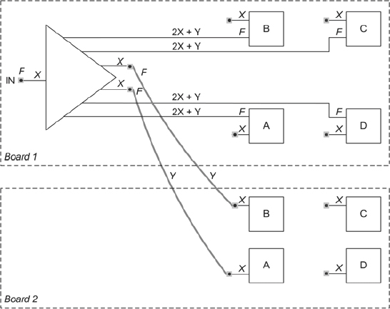
delay, X and Y, which are used as fundamental values during the board design. Y is the delay of typical clocks along a particular standard length co-axial cable with high-quality shielding and co-axial connectors which is mass produced and used widely in HAPS-based platforms. Having a single type and length of cable with relatively constant delay meant that the on-board traces can be designed to the same value Y. It is a small matter for PCB designers to delay match traces on the board, although the zig-zag trace routing employed may increase the need for extra board routing layers. The other quantum of delay, X, is the stub delay to and from FPGA pins and nearby connectors and is relatively simple to keep constant. The values for X and Y will be characteristic for a given family of boards, for example, for one family of boards, X= 0.44ns and Y = 1.45ns. With care, the values of X and Y can be maintained across new board designs in order to allow easier mixing of legacy and new boards in the same prototype.
We can now see from the diagram that clock delay between the clock source and any of the FPGA clock pins will be the same value, 2X+Y, i.e., 2.33ns for our HAPS example, and thus we have minimized clock skew across the partition.
Note, however, that the received FPGA clocks, although mutually synchronized, will not be in sync with the master clock input, F. If we wish to use F and its distributed derivatives, then we will need to employ phase-locked loops, which we will now discuss.
5.3.2. Phase-locked loops (PLL)
PLLs are extremely useful for removing insertion delay in cross-board clock networks, for example, to reduce clock skew between different parts of the prototype. Figure 52 shows a board-level PLL driving four FPGAs. As above, with the use of trace-length matching, the stubs at each FPGA clock input and the stubs at the PLL outputs can be made equal to the value X. Over many board manufacturing runs, the absolute value of X may vary but will be consistent enough for any given board.
Figure 52: PLL used to re-align FPGA clocks
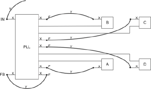
We see also that the FPGAs are linked to the PLL outputs by equal length cables or delay Y. Co-axial cables and high-fidelity clock connections are highly recommended for best reliability and performance. We can see that the on-board delays from PLL to each FPGA are matched.
For providing the necessary clock resources at the top-level of the “Super-FPGA,” the board should include PLL capabilities, which are useful for a number of tasks. Although the FPGAs used may include their own PLL features, the boards should include discrete PLL devices such as those available commercially from numerous vendors.
5.3.3. System clock generation
The clock generation and its flexibility are critical to the reliable operation of a multi-FPGA Prototyping system. Some of these capabilities must be implemented at the board level, but others must make use of the available clock resources within the FPGAs. It is therefore important that from the beginning we understand the available clocking resources on the chosen FPGA. As mentioned in chapter 3, FPGA devices today have very capable clocking capabilities including DLLs, PLLs, clock multiplexers and numerous global and regional clocks across various regions of the FPGA fabric.
Once the available clocking resources in the FPGAs are understood, we should determine what additional external clock sources and routing will properly exploit them and maintain the most flexibility for all future applications.
The following is a list of recommended considerations:
- Where is the clock sourced?
o Generated locally on main board.
o External source to the main board.
o Generated in FPGA.
- What clock rates are required?
o Estimate the range of possible FPGA clock frequencies.
o Plan to generate an arbitrary clock rate, with fine granularity.
- What clock skew can be tolerated?
o Inter-FPGA synchronization: make sure all FPGAs receive the clock sources at an acceptable skew.
o Inter-board synchronization: in large systems, make sure all clocks arrive at all FPGAs with an acceptable skew.
In addressing the above considerations, an in-house board might typically include most or all of the following elements:
- On-board clock synthesis: typically a PLL driven by a crystal oscillator reference with configurable parameters to select the desired clock frequency. To increase the flexibility the crystal oscillator may be removable. Multiple clocks generators may be needed to support systems with multiple clocks.
- Input clock source selector: given the multiple sources from which clocks can be sourced e.g., local (on board, FPGAs), or external, a clock source multiplexer should be implemented. Management of the multiplexer could be by manual switches or programmed by a separate software utility (see section 5.4 below).
- Clock distribution: regardless of the clock source, clock distribution must ensure the clock is distributed to local and external consumers with an acceptable skew. Excessive skew may result in improper logic propagation and decrease the timing margins between two or more entities passing synchronous signals to each other. On-board and connector delays must be accounted for and equalized while maintaining acceptable signal quality.
- External clock source: propagation delay from one board to another must be accounted for and propagation delays should be equalized by appropriate phase shifting. Special attention must be paid to a situation where multiple PLLs are cascaded between the source and destination of the clock path, as instability and loss of lock may occur if not properly designed.
- Special high-speed clocks: in addition to the application clocks, there may be a need for high-speed clocks to multiplex multiple signals on one pin. This is typically used when the number of signals between two FPGAs is greater than the number available pins between them. Using a high-speed clock the signals can be time-multiplexed over a single pin at the source and are then de-multiplexed at the receiving end. For this scheme to work properly both sides of the interface must have the same high-speed clock with minimal skew. Some prototyping tools such as Synopsys’ CPM (Certify Pin Multiplier) assist the use of this technique.
- Clock scaling: Flexibility in clocking requires that the top-level clocks can be scaled to the correct frequencies for various parts of the design. Although dividers and other logic resources can be used for this inside the FPGA devices, PLLs also have their role to play.
5.4. Clock control and configuration
With the options discussed above, it is clear that the clock configuration of our board could become rather complicated. A large number of switches may be necessary to fully cover all the clocking options on a sophisticated multi-FPGA board. Nevertheless, with good documentation and the correct training, a board with such clocking flexibility would be more likely to be re-usable over multiple projects.
Alternatively, we might use programmable switches under the control of an onboard hosted microcontroller, or a utility running on an external host PC, as we shall explore in chapter 6.
5.5. On-board Voltage Domains
SoC designs use an increasingly complex collection of voltages both for interfacing with external components and in an internal hierarchy of voltage islands in order to reduce power (see the ARM®-Synopsys Low-Power Methodology Manual, LPMM, in the bibliography for further detail). The internal voltage islands are usually inferred by EDA tools, based on the power-intent captured in side-files written in formats like the universal power format (UPF). Internal voltage islands therefore do not generally appear in the design RTL and do not get mapped onto the FPGA-based prototype. If the RTL delivered to the prototyping team already has voltage control logic, retention registers etc. then these will need to be tied to inactive state (see chapter 7). It is very unlikely that the voltage regions on the FPGA board will correspond with the regions within the SoC itself.
External voltage needs must still be mapped correctly, however. FPGA IO pins are arranged in banks that support different voltage thresholds and are powered by different voltage rings. It is important that the platform can supply any of the required voltages and route them to the relevant FPGA power pins. Voltage inflexibility additionally constrains IO usage and placement so that voltage rather than performance or connectivity sometimes governs partitioning choices with the result of compromising other priorities. Indeed, new voltage requirements can be a reason that existing boards cannot be reused in new projects, so building in flexibility is a good investment for helping to ensure longer life of the boards across multiple projects.
Figure 53 shows a screenshot from a utility which is used to remotely set-up the voltage of different regions on a HAPS-64 board.
Figure 53: On-board IO voltage configuration
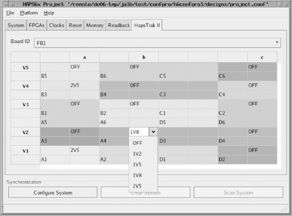
Here we can see that the FPGA pins and daughter-card connectors are grouped the into different regions which can be set to chosen voltages (in reality, there is good use of color to clarify the user interface). The region voltage is slected by use of pull-down menus and we can see that “OFF” is also a valid option.
This configuration tool then configures programmable switches on the board which setup the reference and rail voltage for the FPGA devices themselves. Although this is an example from a commercial board, it is possible to create such utilities in-house and might be worth the effort if many copies of a board are to be made and used in a wide variety of projects.
5.6. Power supply and distribution
When considering the power supply scheme, we need to consider the system’s scalability, worst-case power budget, and planned modularity. For example, a multi-board system allows greater flexibility but the arrangement of the boards and subsystems is impacted by their power requirements.
During system assembly to support daughter boards which draw power from the main board, as shown in the simple example of Figure 54, careful power budgeting for the additional boards must be done. If the combined current consumption on the daughter boards will exceed the available power on the main board, separate power must be supplied to the daughter board from the main external power supply as to not damage the main board supply circuit and possibly the board traces. In addition, to prevent damage to the main board from accidental power short on the daughter board, a current limiting circuit, or a “resettable fuse” should be considered at every power exit point. The connector pins supplying the current should also be properly sized to the expected current draw for reliable and long-term system reliability.
Figure 54: Example of non-recommended power distribution
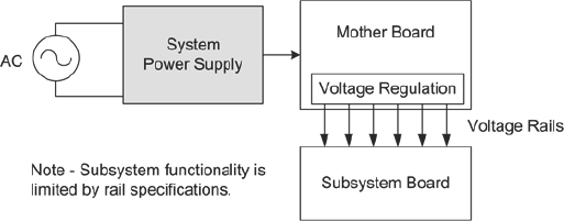
It is bad practice for major sub-system boards to be powered from a host board, especially sub-system boards which mount their own FPGAs. It may be tempting to have voltage regulation and distribution from the host board onto all secondary boards, however, the latter may require current which exceeds the capability of board-to-board connectors carrying the voltage rails. This may be especially apparent during FPGA power-up and configuration, or even during live reset. Momentary brown-out of voltage rails, because of some particular activity of the FPGA, can be a hard problem to diagnose late in the prototyping project.
Figure 55: Example of centralized power distribution
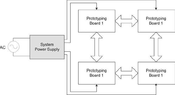
Far more preferable is that each board be specified with its own power input, and voltage regulation and distribution are managed locally. Each board then draws its input power from a common external power supply that is large enough to power all boards in the system as described in Figure 55..
As shown in the diagram, one power supply provides power to each of the boards in the system so it must be capable of sourcing power to all boards combined under worst-case scenario. Estimating the total power consumption is covered in the next section.
5.6.1. Board-level power distribution
Each FPGA board will need a number of voltages depending on the FPGA specifications and user selections:
- Core voltage: used to power the FPGA internal logic, is typically lower than the IO voltage and determined by the FPGA vendor.
- IO voltage: used to power the FPGA pins, and can vary depending on the signaling levels used in the system. IO voltages are typically grouped in banks that share the same IO voltage, so there is a potential to have multiple IO voltages across all IO pins. However, using multiple IO voltages will require multiple “power islands” in the PCB which will complicate the layout design. When selecting signaling levels, we need to consider the implication on IO speed, noise margin and possible interface constraints. All inter-FPGA connectivity can easily use the same signaling standard, but we need to make sure the signaling level on the FPGA side will be compatible with external devices to which the system may be connected.
- IO current: if the requirement of the externally connected device cannot be met using the FPGAs programmable output pin drives of up to 24mA, then we will need to add external buffers between the FPGA IOs and external components, probably mounted on daughter cards. It may only be necessary to add these buffers to a subset of the FPGA pins, if any.
On each board, the power may be supplied by single or multiple voltages, and then lower voltages are generated using power generation circuitry, such as DC/DC converters. Given the multiple possible signaling standards, we may want to allow a certain degree of programmability of the IO voltages.
In estimating the power consumption, we should consider worst-case scenarios as the actual consumption depends on a number factors that may vary and are unknown for any arbitrary design in the future. Specifically, the power needed for each FPGA depends mostly on the switching rate and the number of internal FFs used in a design, so an estimation of these two factors must be made. In addition, IO switching and static current consumption should also be accounted for.
We must take into account initial power up requirements of the system because high current spikes often occur when powering up FPGAs (see chapter 11 for more details). Including all the above considerations, we can see that estimating total power is somewhat statistical but in all cases we should be conservative. To help estimate the power consumption for a given FPGA, vendors typically provide power estimation tools that make it easier to predict the power consumption for each FPGA.
Since core and some IO voltages are considerably lower than device voltages used in the past, the tolerance to variations is proportionately smaller as well. For proper FPGA operation, it is strongly recommended to employ some power monitoring circuits. Such devices will change state when voltage drops below a certain level, often programmable. When power faults occur, an alarm circuit should be triggered to alert the user to them. More about power faults management is described below.
In addition to the FPGA power needs, we should consider making provisions for additional programmable voltage level supplies to be used as reference voltages for auxiliary analog circuits such as ADC and DACs and other auxiliary circuits to be added to the FPGA system.
Recommendation: when connecting multiple boards together, it is safer to allocate a separate power distribution to each rather than have secondary boards which piggy-back onto a prime board. Piggy-back boards, sometimes called daughter boards or mezzanine boards, must meet a limited power spec in order not to overload the power supply of the host board.
5.6.2. Power distribution physical design considerations
The physical delivery of power to FPGAs is very critical to system stability and reliability. Since the FPGAs are the main power consumers, high-speed clocking and large numbers of FFs switching simultaneously will result in large current spikes at the clock edge where most logic changes take place. These current spikes, if not properly supplied, will cause power level drop or noise on the power lines at FPGA power pins and can result in unreliable operation.
To mitigate this potential problem, good low-impedance power planes should be used with adequate amount of continuous copper between the power supply circuit and the FPGA’s power pins. Equally important is the power return path, or ground, so a low-impedance ground to the power supply is also necessary. In addition, large reservoir (100μF) and high-frequency small (.1μF) low-ESR, capacitors should be placed as close as possible to the power pins of the FPGAs in order to smooth the effects of both the slow and fast current surges.
In addition, special attention must be paid to IO power and grounding. Adequate power distribution should be implemented as mentioned above, but also care must be paid to signal groupings and ground pins. Typically, there is a ground pin per a number of IO pins. The number of IO pins per ground pin varies depending on the FPGA. Many pins switching at the same time to/from the same logic levels can result in a large return current through the ground pin. This may cause a “ground bounce,” where the ground reference rises momentarily and may cause incorrect logic interpretation in input pins associated with this ground pin. To mitigate this risk, it is advised to provide an adequate low impedance ground for the ground pins that are between the IO pins, and carefully follow the FPGA manufacturer’s board layout recommendations. In addition, to minimize the return current it is recommended to configure the FPGA IO such that they use the least amount of current drive on output pins rather than full 24mA on all pins by default. This will reduce current while maintaining adequate drive and signal quality.
5.7. System reliability management
As with any other design and test equipment, the reliability of the prototyping system is of critical importance to the user. A reliable system should have built-in protection from faults to the greatest extent possible and provide the user with warnings, should a fault occur. The types of faults typical to such large systems relate to power supply and thermal management.
5.7.1. Power supply monitoring
Proper operating voltage should be supplied to all FPGA and other components by design. However, power supply faults still may occur for variety of reasons, such as main power supply failure, unintended excessive current draw, or even accidental shorts on the power lines.
While such faults cannot be automatically repaired, it’s important the user is aware if such a fault has occurred. Therefore it is recommended that each power supply circuit has a power monitor circuit that continuously measures the voltage level and asserts a fault signal when the voltage is outside the monitoring range.
In addition to the on-board power monitoring, current generation FPGAs have a built-in system monitor circuit that can monitor all on-chip voltages and external voltages, as we shall see below. Since such voltage monitoring circuits are available “for free” in the FPGA it is recommended to use them.
Once a power failure is detected, the system management circuit can do one or all of the following:
- Set a visible indication of the fault, such as an LED. A more sophisticated system may have the fault monitoring circuit linked to a host computer, such that its status can be read by a program available to the user. Such a feature is critical when the system is housed in an enclosure, or located at a remote location away from the user.
- Assert a global reset signal to reduce operating current draw.
- De-configure all FPGAs, to ensure they consume the least amount of power. This will also serve the purpose of alerting a remote user that a system fault has occurred.
5.7.2. Temperature monitoring and management
As FPGA devices became larger and faster, so did their appetite for power, despite the shrinking node geometries. Current generation FPGAs with high utilization levels, running at high clock rates, may generate more heat than their package can dissipate to free air. Overheating die may result in malfunction and may cause irreversible damage to the FPGA and the PCB. In addition, when the prototyping system is enclosed in a box where the ventilation is marginal, FPGA temperature can rise to damaging levels. In either case thermal management circuitry should be considered and thermal requirements must take into account these worst case scenarios.
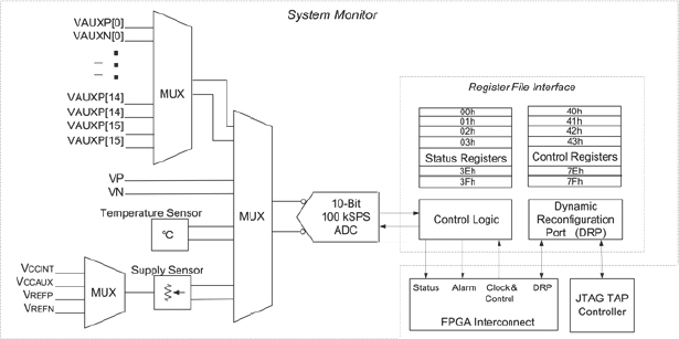
As introduced above, the FPGA’s system monitor” is highly programmable and has multiple modes of operation, but importantly it can also monitor the FPGA die’s average junction temperature. Monitored data is available at the JTAG port and also via the FPGA-resident design if the system mo nitor module is instantiated in the design. This could be a part of the FPGA-specific chip support block mentioned in chapter 4.
Figure 56 shows the system mo nitor circuit available at the core of the Virtex®-5 FPGA. As shown, in addition to the voltage monitoring, the system monitor has a temperature sensor with an associate alarm signal that is activated when the junction temperature exceeds its acceptable level. Such a signal can be used to implement a system-level power and temperature monitoring circuit, and alert the user to a fault in the system.
Figure 56: FPGA System Monitor
Once an over-temperature alarm is set, the system management circuit may do some or all of the following:
- Set a visible alarm, like an LED.
- Turn on fans to remove the excess heat.
- Put the system in reset condition.
- De-configure all FPGAs, to make sure they will consume the smallest amount of power.
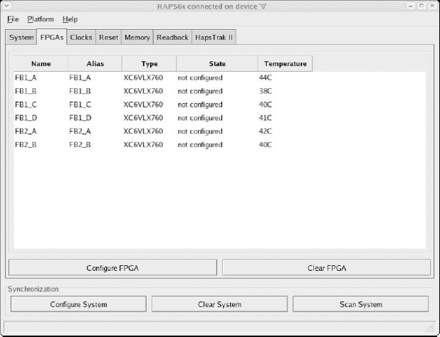
- An example of how temperature could be monitored from a host is shown in Figure 57 . This is a screen shot of a PC-hosted utility called CONFPRO which is connected to a supervisor microcontroller running locally on a HAPS board (actually running on a Microblaze CPU embedded in an FPGA on the board). The screen shows the values read from the system monitors of six Virtex®-6 devices and any mitigation steps in progress e.g., controlling fans mounted on each FPGA. The same microcontroller also controls the FPGA clocks, resets and configuration so each of the above mitigation techniques can be automated locally or under control of the user.
In addition to the on-chip temperature monitoring, it’s recommended the system also includes a number of temperature sensors placed close to where temperature is expected to be higher than other parts of the system, typically close to the FPGAs. Such devices are typically programmable and can produce an alarm signal when temperature is higher than their programmed value. Connecting these devices together and combining them with the on-chip temperature sensors/alarms will create a well monitored system.
Figure 57: monitor in CONFPRO
5.7.3. FPGA cooling
To improve heat dissipation, it’s recommended to install a heat sink to each FPGA. There are many such heat sinks that come with self-adhesive film, so installation is fairly simple. If a heat sink alone is not adequate enough to remove the heat from the FPGAs, a small fan over the heat sink or a fan with a heat sink combination can be placed on each FPGA to significantly improve the heat dissipation. To accommodate these fans, the necessary power supply and connectors should be incorporated into the main board. The fans need not be on all the time but could be controlled by a small loop making use of the FPGA’s temperature monitor.
In the long run, boards run with FPGAs having not heat sink or fan cooling might receive temperature stress and prove to be less reliable.
5.8. FPGA configuration
FPGA configuration is the process in which the FPGAs are programmed with a bit stream and take on our intended functionality. Configuration data, which can range in the tens of Mbits per FPGA, is generated by the FPGA tools after place & route is completed.
Since FPGAs are SRAM-based volatile devices, the configuration process must take place after each power-up, but can also be performed an unlimited number of times after initial configuration.
There are a number of methods to configure FPGAs that can be broadly described as parallel or serial, master or slave, and JTAG. The mode is determined by hardwiring dedicated configuration mode signals. The following list describes the major characteristics of the different configuration modes:
- In the master modes, the FPGA is controlling the configuration upon power-up or when triggered by a configuration pin.
- In slave modes an external device controls the configuration interface.
- Serial configuration is slower than parallel but uses less signals, therefore leaving more signals to be used for the application itself.
- JTAG interface overrides and other configuration modes.
Configuration data can reside in a non-volatile memory or at a host computer. Multiple bit streams can be placed sequentially in the storage device and all FPGAs are configured in order in a sequence determined by hardwiring each FPGA.
The most common configuration mode is via JTAG and this is usually how the download cables form host PC’s communicates with the devices. However, it would be non-intuitive for those not familiar with FPGAs to make use of that download cable approach.
For non-FPGA experts, we can employ some added dedicated circuitry and common CompactFLASH™ (CF) cards. Commercial CF devices are readily available and of high enough capacity to hold the configuration data of even the largest FPGA devices. In fact, multiple configurations can be stored in the same card and the end-users can choose which one is loaded on the board by a simple setting of switches or even by remote control from a utility running on a host PC in the lab. There would still be room left over in the CF memory to hold other data, for example, documentation and user guides. This approach is very popular with those creating multiple copies of the FPGA platform for distribution to remote end-users. Removable CF cards provide the flexibility to transport the systems configuration to remote locations.
To enable the use of CF cards, a dedicated circuit called the Xilinx® System ACE™ controller is typically implemented in a separate small FPGA on the board. System ACE technology is a piece of Xilinx® IP which reads the CF card and then emulates a JTAG interface memory for the FPGAs to be configured. Figure 58 shows a multi-mode configuration approach centered upon the System ACE controller.
Figure 58: CompactFLASH™ based configuration via System ACE™ technology
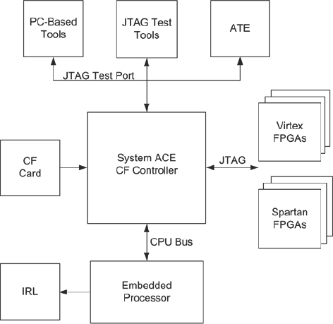
More information about System ACE and for a full description of FPGA configuration modes, refer to Xilinx® documentation listed in the references.
5.9. Signal integrity
As mentioned above, clock skew should be minimized to an acceptable level. The main contributors to clock skew are jitter in the source signal, and noisy power supply and signal environment. To minimize these negative effects, special care must be paid to the signal propagation on the boards and across boards including
- Consistent impedance of all clock signals is critical.
- Proper routing on the board will reduce cross-talk with other signals.
- Well regulated power supplies with low-impedance paths to all loads.
- Trace length and delay matching for most likely parallel data and clock paths e.g., from an FPGA to its dedicated IO connector.
- There are other sources for understanding the issues on board layout and signal integrity (see references). This is not a manual for PCB layout and design and we only mention it here as a reminder that creating a large multi-FPGA board is a challenging problem, although not insurmountable with access to the right PCB-layout expertise.
5.10. Global start-up and reset
Once a system clock generation and distribution scheme is designed, we need to consider the effects of integrating the clocking circuits with the FPGA system. In a mult i-FPGA prototype in particular, it is essential that all FPGAs become operational at the same time i.e., have their resets de-asserted on the same clock edge.
When PLLs are used either on the board and/or inside the FPGAs, the system startup must be delayed from after power-up until all timing circuits (PLLs) are stable and phase locked to their respective sources.
In this case, we employ a global reset circuit that holds the whole system at the reset state until all PLLs in the system are locked. There is more detail on this in chapter 8, however, during board development, it is important to make external PLL device locked an reset signals available at the pins of at least one FPGA so that they might be gated into an overall reset condition tree.
5.11. Robustness
As mentioned in chapter 2, one excellent reason to use FPGA-based prototypes during SoC verification is to allow the design to be taken out of the lab. To enable such use, platforms must be first of all reliable but that is also true of in-lab platforms. For portability, the platform must also be robust enough to survive non-lab conditions. It is important that the platform is able to work as well and as error-free as any other piece of field test equipment.
The platform may be made more robust by using strengthening struts to add rigidity to the board itself, by securing daughter cards using spacers, pillars and screws. The whole assembly may also be held in a strong case or rack but if so, then consideration should be given to maintaining the necessary access to test points, extension card sites and peripheral ports. The case should also provide for the full power and cooling needs of the platform in the field. Early consideration of these points may avoid frequent remedial action when the platforms are in the field or used by others outside the lab, such as software developers, for whom the platform is just a box under their desk and should be as simple and reliable as possible.
We will revisit the subject of robustness in more detail in chapter 12 where we consider how we might take our prototype out of the lab and into the field for various reasons.
5.12. Adopting a standard in-house platform
So far, we have given long consideration of the topology of the platform and its potential for reuse in follow-on projects. R&D centers where FPGA-based prototyping is widely used tend to adopt a standardized connectivity and modularity. Various experienced prototyping teams have adopted a tile-based approach where each new board, at whichever R&D site it was developed, is designed and built to a common form-factor and using common connectors and pin-out. This allows the potential for each board to be reused by other sites, increasing the potential return on that investment. Such a standardized approach does however take considerable co-ordination and management and can lead to constraints on new platforms in order to fit in with the legacy of the standard. As new boards are developed, the choice will often arise between staying within the standard and making a specific departure in order to better meet the needs of the current project. For example, should a given IO socket be added to the platform, even though it would prevent or limit physical connections to other standard modules?
Legacy can also be a significant obstacle during step-changes of in-house design practice, for example, when switching to a new wider SoC bus which may overflow the standard connector interface between boards.
An important part of an in-house standard is the physical connectivity. Tile-based or stack-based arrangements have allowed boards built on the standard to be connected together in a multitude of three-dimensional arrangements. Some of these standard tiles do not have FPGA resources at all but instead hold peripherals or bespoke external interfaces and connecters, for example SCART sockets or IO standard interfaces. This meets the modularity guidelines mentioned earlier in this chapter and aids reuse but distributing components over a large area can have an effect upon overall performance. The authors have seen a number of examples of stacking modular systems where performance and reliability have proved inadequate so the connectors between modules become a critical part of any in-house standard platform. The connectors must not only carry enough signals, they must also have good electrical characteristics, be high-quality and physically robust. Choosing connectors on price will prove to be a false economy in the long run.
Nevertheless, the advantages of an in-house standard are significant when matched with a suitable infrastructure for continued development, distribution, documentation and support. Let’s quickly consider each of these in turn:
- Development: to prevent duplicate development effort, for example multiple but similar boards containing the same FPGA, it is necessary to coordinate FPGA-based prototyping specialists over a number of sites and projects towards supporting and growing the in-house standard. An infrastructure is required which includes a catalog of available boards, their specifications, technical documentation and the roadmap/schedule for new board development.
- Distribution: those entering into new FPGA-based prototyping projects need to be able to specify, source and assemble the required platform quickly from available boards. Only if boards are not immediately or quickly available should a new board development be considered. To make that possible, board developers and manufacturing sources need to have visibility of forthcoming projects so that the necessary boards can be created and put into stock. The management of the in-house standard becomes a sophisticated business within a business. It will take considerable resources to maintain but will reduce reliance on single contributors and help to protect the investment on previous in-house platform development.
- Documentation: the standard itself must be documented and an arbiter appointed to certify the compliance of any new board. Then each individual board should have sufficient documentation to firstly allow other users to decide its suitability for a project but then to fully describe every aspect of its final use. It may also be beneficial to create training material and reference design examples to shorten the learning curve for new users, some of whom will be remote from the original board designers. Insufficient documentation will not only result in delayed projects and inefficient use of the board but also require more help from support personnel.
- Support: the in-house standard will need personnel to support the use of boards within FPGA-based prototyping platforms, often in many sites and projects at the same time. Modern intranet and other internal media make this more possible than even a few years ago but it may still require that large installations of platforms would require accompanying on-site support personnel, depending on platform reliability and ease-of-use. The support infrastructure might be centralized or distributed but must certainly have continuous availability and expertise, minimizing the risk to individual projects of key support resources becoming unavailable. A natural extension of support for the platform is the creation of a central lab for FPGA-based prototyping, offering not only the platform but also the design services, expertise, scheduling and management for the entire project. An SoC team may then choose to outsource the entire FPGA-based prototype as a package of work within the overall SoC project budget and schedule. This has become a popular option for many FPGA-based prototyping projects and falls under the normal rules for economy of scale. It is interesting that there are such centralized design service teams who do not actually make their own boards but instead assemble platforms from ready-made boards from external suppliers.
To summarize, the establishment of an in-house standard platform can require a large investment in time, expertise and personnel. Historically, the scale of this infrastructure has meant that in-house standards were generally only adopted by larger multi-site corporations, performing regular prototyping projects. However, as we shall see in chapter 6, the growth of commercial platform suppliers has meant this infrastructure can be largely outsourced and now reuse and standardization is available to all teams, whether at a corporation or a start-up.