CHAPTER 6 |
WHICH PLATFORM? |
Having spent chapter 5 exploring the detailed considerations in creating an FPGA-based hardware platform for an FPGA-based prototyping project, we will now consider the other side of the so called “make versus buy” argument. When does it make more sense to use a ready-made FPGA board or even a more sophisticated FPGA-based system instead of designing a bespoke board? What interconnect or modularity scheme is best for our needs? What are our needs anyway, and will they remain the same over many projects? The authors hope that this short chapter will compliment chapter 5 and allow readers to make an informed and confident choice between the various platform options.
6.1. What do you need the board to do?
The above subtitle is not meant to be a flippant, rhetorical question. When investigating ready-made boards or systems, it is possible to lose sight of what we really need the board to do; in our case, the boards are to be used for FPGA-based prototyping.
There are so many FPGA boards and other FPGA-based target systems in the market at many different price and performance points. There are also many reasons why these various platforms have been developed and different uses for which they may be intentionally optimized by their developers. For example, there are FPGA boards which are intended for resale in low-volume production items, such as the boards conforming to the FPGA mezzanine card (FMC) standard (part of VITA 57). These FMC boards might not be useful for SoC prototyping for many reasons, especially their relatively low capacity. On the other hand, there are boards which are designed to be very low-cost target boards for those evaluating the use of a particular FPGA device or IP; once again, these are not intended to be FPGA-based prototyping platforms as we describe them in this book but may nevertheless be sold as a “prototyping board.”
Before discriminating between these various offerings, it is important to understand your goals and to weigh the strengths and weaknesses of the various options accordingly.
As discussed in chapter 2, the various goals of using an FPGA board might include:
- Verification of the functionality of the original RTL code
- Testing of in-system performance of algorithms under development
- Verification of in-system operation of external IP
- Regression testing for late-project engineering change orders (ECO)
- In-system test of the physical-layer software and drivers
- Early integration of applications into the embedded operating system
- Creation of stand-alone target platforms for software verification
- Provision of evaluation or software development platforms to potential partners
- Implementing a company-wide standard verification infrastructure for multiple projects
- Trade-show demonstrations of not-yet realized products
- Participation of standards organization’s “plugfest” compatibility events
Each of these goals place different constraints on the board and it is unreasonable to expect any particular board to fulfill optimally all goals listed above. For example, a complex board assembly with many test points to assist in debugging RTL may not be convenient or robust enough for use as a stand-alone software target. On the other hand, an in-house board created to fit the form factor and price required for shipment to many potential partners may not have the flexibility for use in derivative projects.
6.2. Choosing the board(s) to meet your goals
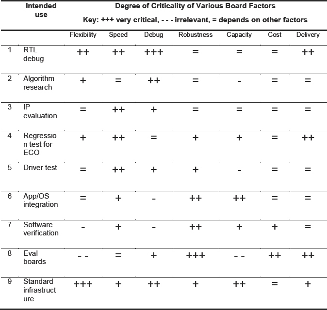
The relative merits of the various prototyping boards are subjective and it is not the purpose of this chapter to tell the reader which board is best. Acknowledging this subjectivity, Table 11 offers one specific suggestion for the weighting that might be applied to various features based on the above goals. For example, when creating a large number of evaluation boards, each board should be cheap and robust. On the other hand, when building a standard company infrastructure for multiple SoC prototyping projects, flexibility is probably more important.
We do not expect everybody to agree with the entries in the table, but the important thing is to assess each offering similarly when considering our next board investment. There are a large number of boards available, as mentioned, and we can become lost in details and literature when making our comparisons. Having a checklist such as that in table 11 may help us make a quicker and more appropriate choice. The column for cost may seem unnecessary (i.e., when is cost NOT important?) but we are trying to warn against false economy while still recognizing that in some cases, cost is the primary concern.
Readers may find it helpful to recreate this table with their own priorities so that all stakeholders can agree and remain focused upon key criteria driving the choice
Table 11: Example of how importance of board features depends on intended use
For the rest of this chapter we will explore the more critical of the decision criteria listed as column headings in Table 11.
6.3. Flexibility: modularity
One of the main contributors towards system flexibility is the physical arrangement of the boards themselves. For example, there are commercial boards on the market which have 20 or more FPGAs mounted on a single board. If you need close to 20 FPGAs for your design, then such a monster board might look attractive. On the other hand, if you need considerably fewer FPGAs for this project but possibly more for the next one, then such a board may not be very efficient. A modular system that allows for expansion or the distribution of the number of FPGAs can yield greater return on investment because it is more likely that the boards will be reused over multiple projects. For example, an eight-FPGA prototype might fit well onto a ten-FPGA board (allowing room for those mid-project enhancements) but using a modular system of two four-FPGA boards would also work assuming extra boards can be added. The latter approach would allow a smaller follow-on project to use each of the four-FPGA boards autonomously and separately whereas attempting to reuse the former ten-FPGA board would be far less efficient.
This exact same approach is pertinent for the IO and peripherals present in the prototype. Just because a design has four USB channels, the board choice should not be limited only to boards that supply that number of channels. A flexible platform will be able to supply any number up to four and beyond. That also includes zero i.e., the base board should probably not include any USB or other specific interfaces but should readily allow these to be added. The reason for this is that loading the base-board with a cornucopia of peripheral functions not only wastes money and board area, most importantly it ties up FPGA pins which are dedicated to those peripherals, whether or not they are used.
In particular, modular add-ons are often the only way to support IP cores because either the RTL is not available or because a sensitive PHY component is required. These could obviously not be provided on a baseboard so either the IP vendor or the board vendor must support this in another way. In the case of Synopsys®, where boards and IP are supplied by the same vendor, some advantage can be passed on to the end user because the IP is pre-tested and available for a modular board system. In addition, as IP evolves to meet next-generation standards, designers may substitute a new add-on IP daughter card for the new standards without having to throw away the rest of the board.
An important differentiator between FPGA boards, therefore, is the breadth of available add-on peripheral functions and ease of their supply and use. An example of a library of peripheral boards can be seen at the online store of daughter cards supplied by Synopsys to support FPGA baseboards. The online store can be seen at www.synopsys.com/apps/haps/index.
In general, end-users should avoid a one-size-fits-all approach to selecting an FPGA-based prototyping vendor because in the large majority of cases, this will involve design, project and commercial compromise. Customers should expect their vendors to offer a number of sizes and types of board; for example, different numbers of FPGAs, different IO interfaces etc. but it is important that they should be as cross-compatible as possible so that choosing a certain board does not preclude the addition of other resources later. The approach also requires that modules are readily available from the vendor’s inventory, as the advantage of modularity can be lost if it takes too long to obtain the modules with which to build your platform.
A critical issue with such a modular approach is the potential for loss of performance as signals cross between the various components and indeed, whether or not the components may even be linked together with enough signals. We should therefore now look closely at the interconnect issues involved in maintaining flexibility and performance.
6.4. Flexibility: interconnect
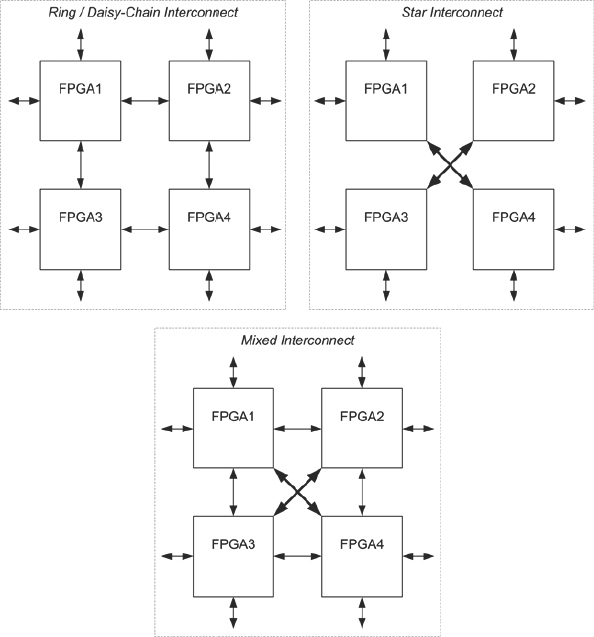
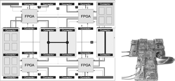
As experienced prototypers will know, the effective performance and capacity of a FPGA-based prototype is often limited by the inter-FPGA connections. There is a great deal of resource inside today’s FPGAs but the number of IO pins is limited by the package technology to typically around 1000 user IO pins. The 1000 pins need then be linked to other FPGAs or to peripherals on the board to make an interconnect network which is as universally applicable as possible, but what should that look like? Should the pins be daisy-chained between FPGAs in a ring arrangement or should all FPGA pins be joined together in a star? Should the FPGAs be linked only to adjacent FPGAs, or should some provision be made to link to more distant devices? These options are illustrated in Figure 59.
There are advantages and disadvantages to each option. For example, daisy-chained interconnect requires that signals be passed through FPGAs themselves in order to connect distant devices. Such pass-though connections not only limit the pin availability for other signals, but they also dramatically increase the overall path delay. Boards or systems that rely on pass-through interconnections typically run more slowly than other types of board. However, such a board might lend itself to a design which is dominated by a single wide datapath with little or no branching.
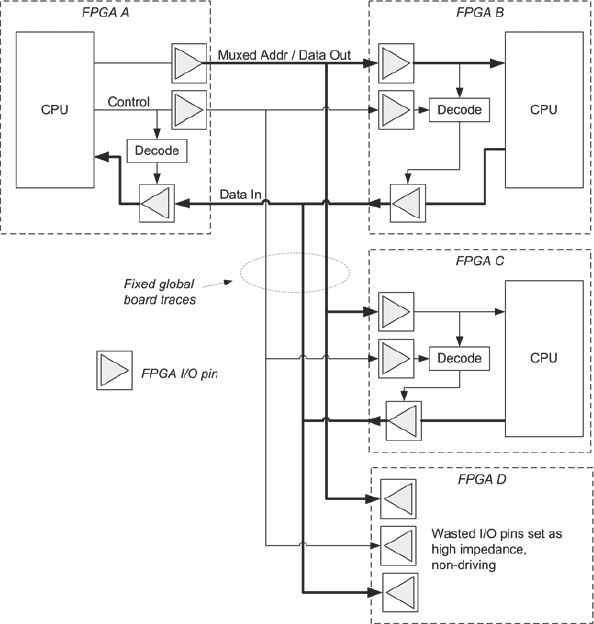
On the other hand, use of a star-connection may be faster because any FPGA can drive any other with a direct wire, but star-connection typically makes the least efficient use of FPGA pins. This can be seen by reconsidering the example we saw earlier in chapter 5, shown here again in Figure 60. Here we see how three design blocks on a simple multiplexed bus are partitioned into three out of the four FPGAs on a board, where the board employs star-based fixed interconnect.
Figure 59: Examples of fixed interconnect configurations found on FPGA boards
The connections between the three blocks are going to be of high-speed, owing to the direct connections, but many pins on the fourth FPGA will be wasted. Furthermore, these unused pins will need to be configured as high-impedance in order to not interfere with the desired signals. If the fourth FPGA is to be used for another part of the design, then this pin wastage may be critical and there may be a large impact on the ability to map the rest of the design into the remaining resources.
Figure 60: Multiplexed bus partitioned into a star-based interconnect.
In the case that a board is designed and manufactured in house, we can arrange interconnect exactly as required to meet the needs of the prototype project. The interconnection often resembles the top-level block diagram of the SoC design, especially when a Design-for-Prototype approach has been used to ease the partitioning of top-level SoC blocks into FPGAs. This freedom will probably produce an optimal interconnect arrangement for this prototyping project but is likely to be rather sub-optimal for follow-on projects. In addition, fixing interconnect resources at the start of a prototyping project may lead to problems if, or when, the SoC design changes as it progresses.
In the same way, a commercial board with fixed interconnect is unlikely to match the exact needs of a given project and compromise will be required. A typical solution found on many commercial boards is a mix between the previously mentioned direct interconnect arrangements, but what is the best mix and therefore the best board for our design?
6.5. What is the ideal interconnect topology?
This brings us back to our decision criteria for selecting boards. Perhaps we are seeking as flexible interconnect arrangement as possible, but with high-performance and one that can also be tailored as closely as possible to meet the interconnect needs of a given prototyping project. Board vendors should understand the compromise inferred by these apparently contradictory needs and they should try to choose the optimal interconnect arrangement which will be applicable to as many end-users’ projects as possible.
Figure 61: Two examples of Indirect Interconnect
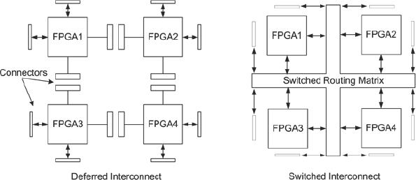
The most flexible solution is to use some form of indirect interconnect, the two most common examples of which are shown in Figure 61. The two examples are deferred interconnect and switched interconnect.
In a deferred interconnect topology, there are relatively few fixed connections between the FPGAs but instead each FPGA pin is routed to a nearby connector. Then other media, either connector-boards of some kind or flexible cables are used to link between these connectors as required for each specific project. For example, in Figure 61 we see a connector arrangement in which a large number of connections could be made between FPGA1 and FPGA4 by using linking cables between multiple connectors at each FPGA. Stacking connectors would still allow star-connection between multiple points if required
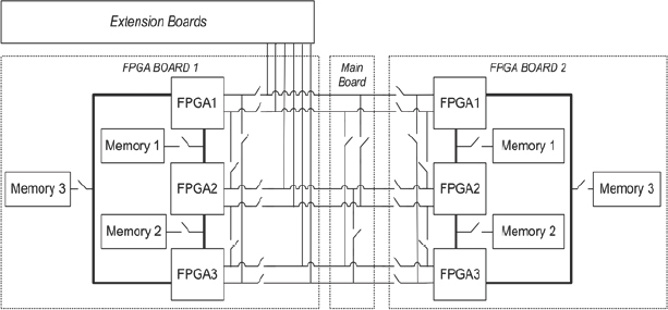
One example of such a deferred interconnect scheme is called HapsTrak® II and is universally employed on the HAPS® products, created by the Platform Design Group of Synopsys at its design centre in Southern Sweden.
A diagram and photograph of a HAPS-based platform is seen in Figure 62, showing local and distant connections made with mezzanine connector boards and ribbon cables.
Figure 62: Synopsys HAPS®: example of deferred interconnect
The granularity of the connectors will have an impact on their flexibility, but deferred interconnect offers a large number of possibilities for connecting the FPGAs together and also for connecting FPGAs to the rest of the system. Furthermore, because connections are not fixed, it is easy to disconnect the cables and connector boards and reconnect the FPGAs in a new topology for the next prototyping project.
The second example of indirect interconnect is switched interconnect, which relies on programmable switches to connect different portions of interconnect together. Of course, it might be possible to employ manual switches but the connection density is far lower and there is an increased chance of error. In the Figure 61 example, we have an idealized central-switched routing matrix which might connect any point to any point on the board. This matrix would be programmable and configured to meet the partitioning and routing needs for any given design. Being programmable, it would also be changed quickly between projects or even during projects to allow easy exploration of different design options. For remote operation, perhaps into a software validation lab at another site, a design image can be loaded into the system and the switched interconnect configured without anybody needing to touch the prototype itself.
In reality, such a universal cross-connect matrix as shown in Figure 61 is not likely to be used because it is difficult to scale to a large number of connections. Vendors will therefore investigate the most flexible trade-off between size, speed and flexibility in order to offer attractive solutions to potential users. This will probably involve some cascading of smaller switch matrices, mixed with some direct interconnections.
Another significant advantage of a switched interconnect approach is that it is very quick and easy to change, so that users need not think of the interconnect as static but something rather more dynamic. After the design is configured onto the board(s), it is still possible to route unused pins or other connections to other points, allowing, for example, quick exploration of workarounds or debug scenarios, or routing of extra signals to test and debug ports. In sophisticated examples, it is also possible to add debug instrumentations and links to other verifications technologies, such as RTL simulation. These latter ideas are discussed later in this section.
Figure 63: Switched interconnect matrix in CHIPit prototyping system
One further advantage of switched interconnect is that the programming of the switches can be placed under the control of the design partitioning tool. In this case, if the partitioner realizes that, to achieve an optimum partition, it needs more connections between certain FPGAs, it can immediately exercise that option while continuing the partitioning task with these amended interconnect resources. In these scenarios, a fine-grain switch fabric is most useful so that as few as necessary connections are made to solve the partitioning problem, while still allowing the rest of the local connections to be employed elsewhere.
Examples of such a switched interconnect solution are provided by the CHIPit® systems created in the Synopsys Design Centre in Erfurt, Germany. A CHIPit system allows the partitioner to allocate interconnections in granularity of eight paths at a time. An overview diagram of a CHIPit system switch-fabric topology is shown in Figure 63. Here we can see that in addition to fixed traces between the FPGAs on the same board, there are also programmable switches which can be used to connect FPGAs by additional traces. Similar switches can link memory modules into the platform or link to other boards or platforms, building larger systems with more FPGAs. Not all combinations of switches are legal and they are too numerous to control manually in most cases, therefore they are configured automatically by software, which is also aware of system topology and partition requirements
6.6. Speed: the effect of interconnect delay
It should be mentioned that the disadvantage of either of the indirect interconnect methods mentioned above is that the path between FPGA pins is less than ideal for propagating high-speed signals. In general, the highest performance path between two pins will be that with the lowest number of discontinuities in the path. Every additional transition such as a connector, solder joint and even in-board via adds some impedance which degrades the quality of the signal and increases its overall opportunity for crosstalk between signals. Upon close analysis, however, we find that this is not such a large problem as may be thought.
For the fastest connections, flight time is low and the majority of interconnect delay is in the FPGA pins themselves. It takes longer for signals to get off-chip and then on-chip than it takes them to travel across the relevant board trace. As prototype boards and the designs running on them become faster, however, this path delay between FPGAs will need to be mitigated in some way to prevent it from becoming critical. For that reason, Synopsys has introduced an automated method for using the high-speed differential signaling between FPGAs, employing source-synchronous paths in order to allow faster speed between FPGAs. We will discuss this techno logy a little further later in chapter 8.
Each of the indirect interconnect approaches adds some delay to the path between the FPGA pins compared to direct interconnect, but how significant is that? If we analyze the components of the total delay between two points in separate FPGAs, using three types of interconnect, then we discover paths resembling those in Figure 64.
Figure 64: Comparing path delays for different interconnect examples
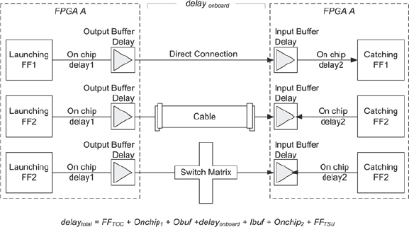
Readers may argue that the FFs should be implemented in the IO pads of the FPGA. This is true, however, it is often not possible to do this for all on-chip/off-chip paths and so the worst-case path between two FPGAs may be non-ideal and actually starting and/or ending at internal FFs.
In this analysis, the path delay is given by the expression shown also in Figure 64. Common to each of the interconnect methods is a component of delay which is the total of all in-chip delays and on-chip/off-chip delays, expressed as:
Σ FFTOC, FFTSU,Onchip1,Onchip2,Obuf, Ibuf
where …
FFTOC is the clock-to-output delay of the launching FF
FFTSU is the set-up time of the catching FF
Onchip1,2 are the routing delays inside the relevant FPGAs
Obuf is the output pad delay of the first FPGA
Ibuf is the input pad delay on the second FPGA
Using figures from a modern FPGA technology, such as the Xilinx® Virtex®-6 family, these delays can be found to total around 4.5ns. This time will be common to all the interconnect arrangements so we now have a way to qualify the impact of the different interconnects on overall path delay i.e., how do the different on-board components of the paths compare to this common delay of 4.5ns?
Firstly, direct interconnection on a well-designed high-quality board material results in typical estimates for delayonboard, of approximately 1ns. We can consider this as the signal “flight time” between FPGA pins. So already we see that even in direct interconnect, the total delay on the path is dominated by factors other than its flight time. Nevertheless, maximum performance could be as high as 250MHz if partitioning can be achieved which places the critical path over direct interconnect.
Deferred interconnect via good-quality cables or other connecting media, using highest quality sockets, results in typical flight time of approximately 4ns, which is now approximately the same as the rest of the path. We might therefore presume that if we use deferred interconnect and the critical path of a design traverses a cable, then the maximum performance of the prototype will be approximately half that which might be achieved with direct interconnect, i.e., approximately 125MHz instead of 250MHz.
However, raw flight time is seldom the real limiting factor in overall performance.
Supporting very many real-life FPGA-based prototyping projects over the years at Synopsys, we have discovered that there are performance-limiting factors beyond simple signal flight time. Commonly the speed of a prototype is dependent on a number of other factors as summarized below:
- The style of the RTL in the SoC design itself and how efficiently that can be mapped into FPGA
- Complexity of interconnection in the design, especially the buses
- Use of IP blocks which have no FPGA equivalent
- Percentage utilization of each FPGA
- Multiplexing ratio of signals between FPGAs
- Speed at which fast IO data can be channeled into the FPGA core
Completing our analysis by considering switched interconnect, we see that the delay for a single switch element is very small, somewhere between 0.15ns and 0.25ns, but the onboard delays to get to and from the switch must also be included, giving a single-pass flight time of approximately 1.5ns, best-case. In typical designs, however, flight time for switched interconnect is less easy to predict because in order to route the whole design, it will be necessary for some signals to traverse multiple segments of the matrix, via a number of switch elements. On average there are two switch traversals but this might be as high as eight in extreme case of a very large design which is partitioned across up to 20 FPGA devices. To ensure that the critical path traverses as few switches as possible, the board vendor must develop and support routing optimization tools. Furthermore, if this routing task can be under the control of the partitioner then the options for the tools become almost infinitely wider. Such a concurrent partition-and-route tool would provide the best results on a switched interconnect-based system so once again we see the benefit of a board to be supplied with sophisticated support tools.
Returning to our timing analysis, we find that a good design partition onto a switched interconnect board will provide typical flight times of 4ns, or approximately the same as a cable-based connection on a deferred interconnect board, once again providing a top-speed performance over 100MHz. The results of the above analysis are summarized in Table 12.
Table 12: Comparing raw path speed for different interconnect schemes.
| Interconnect | Flight Time | Total Path | approx. Fmax |
| Direct | 1ns | 5.5ns | 180MHz |
| Deferred | 4ns | 9.5ns | 105MHz |
| Switched | 4ns | 9.5ns | 105MHz |
6.6.1. How important is interconnect flight time?
In each of the above approximations, the performance of a prototype is assumed to be limited by the point-to-point connection between the FPGAs, but how often is that the case in a real project?
Certainly, the performance is usually limited by the interconnect, but the limit is actually in its availability rather than its flight time. In many FPGA-based prototyping projects, partitioning requires more pins than are physically provided by any FPGA and so it becomes necessary to use multiplexing in order to provide enough paths. For example, if the partition requires 200 connections between two particular FPGAs when only 100 free connections exist, then it doesn’t matter if those 100 are direct or via the planet Mars; some compromise in function or performance will be necessary. This compromise is most commonly achieved by using multiplexing to place two signals on each of the free connections (as is discussed below). A 2:1 multiplexing ratio, even if possible at maximum speed on the 100 free connections, will in effect half the real system performance as the internal logic of the FPGAs will necessarily be running at half the speed of the interconnect, at most.
An indirect interconnect board will provide extra options and allow a different partition. This may liberate 100 or more pins which can then be used to run these 200 signals at full speed without multiplexing. This simple example shows how the flexibility of interconnect can provide greater real performance than direct interconnect in some situations and this is by no means an extreme example. Support for multiplexing is another feature to look for in an FPGA board; for example, clock multipliers for sampling the higher-rate multiplexed signals.
In the final case above, real-time IO is an important benefit of FPGA-based prototyping but the rest of the FPGA has to be able to keep up! This can be achieved by discarding some incoming data, or by splitting a high-speed input data stream into a number of parallel internal channels, For example, splitting a 400MHz input channel into eight parallel streams sampled at 50MHz. Fast IO capability is less valuable if the board or its FPGAs are sub-performance.
These limiting factors are more impacted by interconnect flexibility than by flight time, therefore, in the trade-off between speed and flexibility, the optimum decision is often weighted to wards flexibility.
Summarizing our discussion on interconnect, the on-chip, off-chip delays associated with any FPGA technology cannot be avoided, but a good FPGA platform will provide a number of options so that critical signals may be routed via direct interconnect while less critical signals may take indirect interconnect. In fact, once non-critical signals are recognized, the user might even choose to multiplex them onto shared paths, increasing the number of pins available for the more critical signals. Good tools and automation will help this process.
6.7. Speed: quality of design and layout
As anyone that has prototyped in the past will attest, making a design run at very high speed is a significant task in itself, so we must be able to rely on our boards working to full specification every time. If boards delivered by a vendor show noticeable difference in performance or delay between batches, or even between boards in the same batch, then this is a sign that the board design is not of high quality.
For example, for an interface to run at speeds over 100MHz, required for native operation of interfaces such as PCIe or DDR3, the interface must have fast pins on its FPGAs and robust design and layout of the PCB itself. To do this right, particularly with the latest, high pin-count FPGAs, requires complex board designs with very many layers. Very few board vendors can design and build 40-layer boards for example. The board traces themselves must be length and impedance matched to allow good differential signaling and good delay matching between remote synchronous points. This will allow more freedom when partitioning any given design across multiple FPGAs.
This need for high-quality reproducible board performance is especially true of clock and reset networks, which must not only be flexible enough to allow a wide variety of clock sources and rates, they must also deliver good clock signal at every point in a distributed clock network.
Power supply is also a critical part of the design, and low impedance, high-current paths to the primary FPGA core and IO voltage rail pins are fundamental to maintaining low noise, especially on designs which switch many signals between FPGAs on every clock cycle.
On first inspection, two boards that use the same FPGAs might seem to offer approximately the same speed and quality but it is the expertise of the board vendor that harnesses the raw FPGA performance and delivers it reliably. For example, even device temperature must be monitored and controlled in order to maintain reliability and achieve highest performance possible within limits of the board fabric. Let us look at another aspect of performance, that of trading off interconnect width versus speed using multiplexing.
6.8. On-board support for signal multiplexing
The concept of time division multiplexing (TDM) and its ability to increase effective IO between FPGAs is well understood and it is not difficult to see how two or more signals may share the same interconnect path between FPGA pins. The TDM approach would need mux and de-mux logic inside the FPGA and would need a way to keep the two ends synchronized. It is also necessary to run the TDM paths at a higher rate than the FPGA’s internal logic, and also ensure that signals arriving at the mux or leaving the de-mux both meet the necessary timing constraints. This would be a complex task to perform manually, so EDA tools have been developed that can insert TDM logic automatically, analyze timing and even choose which signals to populate the muxes with. The prime example of such an EDA tool is the Certify® tool from Synopsys, which supports a number of different asynchronous and asynchronous models for TDM.
Whichever tool is used, the problem still exists that with muxing employed, either the overall FPGA-based prototype must run at a lower speed or the on-board paths must be able to run at a higher speed. TDM ratios of 8:1 or higher are not uncommon, in those cases, a design which runs at 16MHz inside the FPGAs must be either scaled back to 2MHz (which is hardly better than an emulator!) or the external signals must be propagated between the FPGAs at 128MHz or greater, or some compromise between these two extremes. With the need for high multiplexing ratios in some FPGA-based prototypes, the overall performance can be limited by the speed at which TDM paths can be run. A good differentiator between boards is therefore their ability to run external signals at high speed and with good reliability; a noisy board will possibly introduce glitches into the TDM stream and upset the synchronizations between its ends.
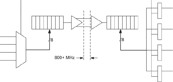
Beyond simple TDM, it is becoming possible to use the LVDS (low voltage differential signaling) capability of modern FPGA pins in order to run on-board paths at speeds up to 1GHz. This full speed requires very good board-level propagation characteristics between the FPGAs. Figure 65 gives a non-detailed example of a serial TDM arrangement, which allows eight signals to be transferred across one pair of differential signals (further detail in chapter 8).
At a high transmission speed of 800MHz and a multiplexing ratio of 8:1, the128MHz speed in our previous example could easily be supported, and even increased to a ratio of 40:1, as long as the board is good enough. The possibility to run much higher mux ratios gives a large increase in the usable connectivity between FPGAs. For example, a TDM ratio of 64:2 (2 rather than 1 because of the differential pins required) could be supported on prototypes running at 30MHz or more, making it much easier for the EDA tools to partition and map any given design. There is more on the discussion of TDM in chapter 8.
Figure 65: High Speed TDM using differential signaling between FPGAs
So, once again, a good differentiator between FPGA boards is their ability to support good quality LVDS signaling for higher overall performance and to supply the necessary voltage and IO power to the FPGAs to support LVDS. It is also important that designers and indeed the tools they employ for partitioning understand which board traces will be matched in length and able to carry good quality differential signals. A good board will offer as many of such pairs as possible and will offer tool or utility support to allocate those pairs to the most appropriate signals. For example, the HAPS-60 series boards from Synopsys have been designed to maximize opportunity for LVDS-based TDM. Details of LVDS capability in each Virtex-6 device and signal routing on the HAPS-60 board is built into the Certify tools to provide an automated HSTDM (high-speed TDM) capability. This example again underlines the benefit of using boards and tools developed in harness.
6.9. Cost and robustness
Appendix B details the hidden costs in making a board vs. using a commercial off-the-shelf board including discussions about risk, wastage, support, documentation and warranty. The challenges of making our own boards will not be repeated here but it is worth reminding ourselves that these items apply to a greater or lesser degree to our choice of commercial boards too, albeit, many are outsourced to the board provider.
We should recall that total cost of ownership of a board and its initial purchase price are rather different things. Balanced against initial capital cost is the ability to reuse across multiple projects and the risk that the board will not perform as required. It may not be sensible to risk a multi-year, multi-million dollar SoC project on an apparently cheap board.
Of particular note is the robustness of the boards. It is probable that multiple prototype platforms will be built and most may be sent to other end-users, possibly in remote locations. Some FPGA-based prototyping projects even require that the board be deployed in situ in an environment similar to the final silicon e.g., in-car or in a customer or field location. It is important that the prototyping platform is both reliable and robust enough to survive the journey.
Recommendation: boards which have a proven track record of off-site deployment and reliability will pay back an investment sooner than a board that is in constant need of attention to keep it operational. The vendor should be willing to warranty their boards for immediate replacement from stock if they are found to be unreliable or unfit for use during any given warranty period.
6.9.1. Supply of FPGAs governs delivery of boards
Vendors differentiate their boards by using leading-edge technology to ensure best performance and economies of scale. However, these latest generation FPGAs are typically in short supply during their early production ramp-up, therefore, a significant commercial difference between board vendors is their ability to secure sufficient FPGA devices in order to ensure delivery to their customers. While some board vendors may have enough FPGAs to make demonstrations and low volume shipments, they must generally be a high-volume customer of the FPGA vendors themselves in order to guarantee their own device availability. This availability is particularly important if a prototyping project is mid-stream and a new need for boards is recognized, perhaps for increased software validation capability.
6.10. Capacity
It may seem obvious that the board must be big enough to take the design but there is a good deal of misunderstanding, and indeed misinformation, around board capacity. This is largely driven by various capacity claims for the FPGAs employed.
The capacity claimed by any vendor for its boards must be examined closely and questions asked regarding the reasoning behind the claim. If we blindly accept that such-and-such a board supports “20 million gates,” but then weeks after delivery find that the SoC design does not fit on the board, then we may jeopardize the whole SoC and software project.
Relative comparison between boards is fairly simple, for example, a board with four FPGAs will hold twice as much design as a board with two of the same FPGAs. However, it is when the FPGAs are different that comparison becomes more difficult, for example, how much more capacity is on a board with four Xilinx® XC6VLX760 devices compared with a board with four XC6VLX550T devices? Inspecting the Xilinx® datasheets, we see the figures shown in Table 13.
Table 13: Comparing FPGA Resources in different Virtex®-6 devices
| FPGA Resource | XCE6VLX550T | XC6VLX760 | Ratio 760:550 |
| logic cells | 549,888 | 758,784 | 138% |
| FF | 687,360 | 948,480 | 138% |
| BlockRAM (Kbit) | 22,752 | 25,920 | 114% |
| DSP | 864 | 864 | 100% |
| GTX Transceivers | 36 | 0 | n/a |
We can see that, in the case of logic cells, the LX760-based board has 38% more capacity than the LX550T-based board, but with regard to DSP blocks, they are the same. There is another obvious difference in that the 550T includes 36 GTX blocks but the LX760 does not have the GTX feature at all.
Which is more important for a given design, or for future expected designs? The critical resource for different designs may change; this design may need more arithmetic but the next design may demand enormous RAMs. Readers may be thinking that visibility of future designs is limited by new project teams often not knowing what’s needed beyond perhaps a 12-month window. For this reason, it is very helpful for prototypers to have a place at the table when new products are being architected in order to get as much insight into future capacity needs as possible. This is one of the procedural recommendations given in our Design-for-Prototyping manifesto in chapter 9.
Getting back to current design, we should always have performed a first-pass mapping of the SoC design into the chosen FPGA family, using the project’s intended synthesis tool in order to get a “shopping list” of required FPGA resources (as discussed in chapter 4).
Project success may depend on other design factors but at least we will be starting with sufficient total resources on our boards. We may still be tempted to use partitioning tools and our design knowledge in order to fit the design into four FPGAs at higher than 50% utilization, but we should beware of false economies. The advice that some find difficult to accept is that economizing on board capacity at the start of a project can waste a great deal of time later in the project as a growing design struggles to fit into the available space.
Recommendation: in general, ignore the gate count claims of the board vendor and instead run FPGA synthesis to obtain results for real resource requirements. We should add a margin onto those results (a safe margin is to double the results) and then compare that to the actual resources provided by the candidate board.
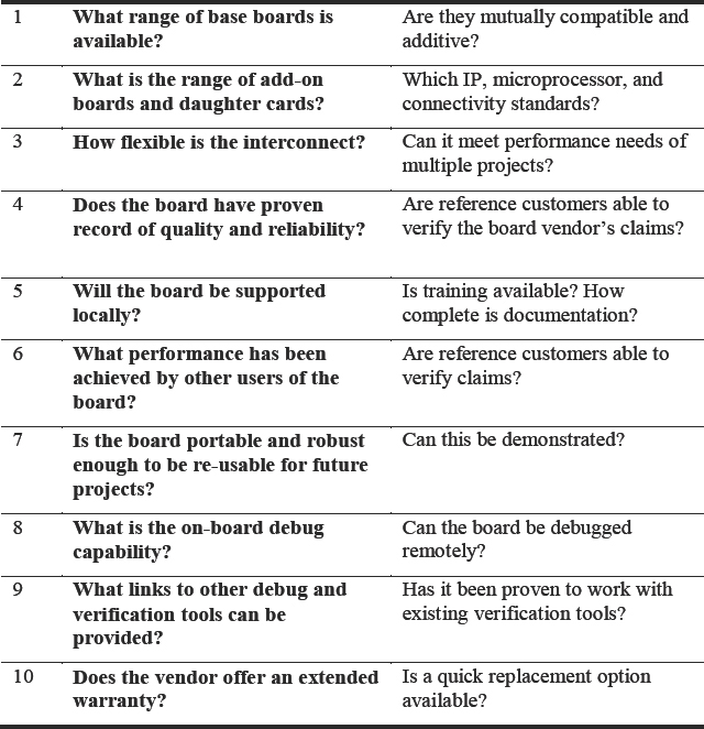
6.11. Summary
Choosing FPGA boards is a critical and early decision in any FPGA-based prototyping project.
A wrong decision will add cost and risk to the entire SoC project. On the face of it, there are many vendors who seem to offer prototyping boards based on identical FPGAs. How might the user select the most appropriate board for their project? The checklist list in Table 14 summarizes points made during this chapter and can help.
Table 14: A top-10 checklist for assessing FPGA prototyping boards
It is important to remember that a prototyping project has many steps and choosing the board, while important, is only the first of them.