CHAPTER 9 |
DESIGN-FOR- |
Having spent the previous chapters covering ways to account for the three laws of prototyping to configure an SoC design for a prototype, we shall now discuss ways that we might have avoided a lot of that work in the first place.
Some of the “Design-for-Prototyping” ideas in this chapter are purely technical in scope, from general and specific styles for writing our original SoC RTL up to architecture-level decisions, all with the intent of making the design more “FPGA-friendly.” Other ideas are more organizational or procedural and will hopefully provoke useful discussion amongst verification and implementations teams alike.
By employing these Design-for-Prototyping guidelines, the prototype will be easier and its verification benefits derived sooner. In effect, we are trying to obsolete the third law of prototyping, i.e., that SoC designs are FPGA-hostile.
9.1. What is Design-for-Prototyping?
Design-for-Prototyping is the art of considering the prototype early in the design process, and establishing procedural and design specific techniques to ease the development of the prototype in conjunction with all other program goals.
There’s an old expression which says that “if a job is worth doing, it is worth doing well.” If we are to employ FPGA-based prototyping in our SoC projects then we should help the prototypers to do the best job possible. We can do that by making some small changes in the SoC design style and overall project procedures, all of which are at least low impact on the rest of the SoC design flow and in fact, many are good design practice for the SoC anyway.
It should be clear from the earlier discussions that putting an SoC design into a prototyping system requires some planning in order to best accomplish the prototyping goals with minimal effort. The aim of this chapter is to help collect many of the recommendations mentioned throughout this book into a single manifesto on how we might make the prototyping tasks simpler and the project more successful. As a result, newcomers to FPGA-based prototyping will better understand how to modify their design style and development procedures to incorporate this methodology. This chapter will present some guiding principles for that change; perhaps best described as a “manifesto for Design-for-Prototyping”.
The decision to add FPGA-based prototyping to the chip design flow should be seen as a change from previous practices rather than a “bolt-on” parallel step. We should expect some impact to all groups in the design team, including SoC designers, verification engineers, software development teams and FPGA platform specialists. Earlier chapters have presented the positive returns expected to the design project as the team embraces this new methodology. Consider Design-for-Prototyping as the investment made to maximize those returns.
The following sections focus on specific RTL coding style practices and organizational (or procedural) guidelines to achieve this overarching goal.
9.1.1. What’s good for FPGA is usually good for SoC
FPGA designs tend to require clean architectures and generic logic for effective synthesis and mapping to the target technology. SoC design processes allow the flexibility of more ad hoc design styles, which may be used inappropriately by some designers to the detriment of subsequent rework.
The need to share a single RTL design for both FPGA and SoC technologies can motivate designers to follow cleaner design styles for simple functionality and reserve unusual coding style for odd cases where it is justified. This path is really the least work for everyone and should benefit the on-going maintenance of the SoC design as a by-product of supporting the FPGA prototype.
The next sections expand on this point with specific coding style suggestions, like FFs at block boundaries, isolation of clock management, and so forth. The whole SoC project should stick to these coding styles, reinforced through formal design reviews and informal organizational behavior. It should be the aim of management and other senior team members who realize the benefits of FPGA-based prototyping to fully embrace the methodology. A “bolt-on” approach to prototyping without a proper integration into the SoC design flow will not yield as great a return on the investment.
9.2. Procedural guidelines
In this section, we outline several important organizational considerations for the prototyping program. There are, of course, many options as to the organizational reporting structure of the prototyping team, however, there should be careful consideration in how the prototyping team’s integration into the organization (and other procedural decisions) affects communication between the design, software, verification, and prototyping teams. Moreover, every effort should be made to integrate and formalize the dataflow and unify the databases, regression, and engineering changes.
Table 22 gives a short summary of the key procedural guidelines that we will cover during this chapter.
Table 22: Procedural recommendations in Design-for-Prototyping
| Recommendation | Comment |
| Integrate RTL team and prototypers. | Have prototyping team be part of RTL design team, trained on same tools and if possible co-located. |
| Prototypers work with software team. | The software engineers are most common end-users for working prototypes. |
| Have prototype progress included in verification plan. | Branch RTL for prototype use only at pre-agreed milestones avoiding many incremental RTL dumps. |
| Keep prototype-compatible simulation environment. | At various points in the prototyping project it helps to compare results with original SoC simulations. |
| Clear documentation and combined revision control. | Track software and RTL changes for prototyping together using same source control. |
| Adopt company-wide standard for hardware and add-ons. | Common hardware approach avoids waste and encourages reuse. |
| Include Design-for-Prototyping in company RTL coding standards. | Most RTL style changes which make prototyping easier are also good for SoC design in general. |
The guidelines focus on managing the communication between the different teams during the whole project, including the prototypers as core members of the project from the start of the project (when architectural trade-offs design goals are first being considered).
9.2.1. Integrate RTL team and prototypers
The success of the overall project is going to be improved if everyone can embrace the idea that there is one design with two target technologies. In addition to FPGA skills, the engineers assigned to the prototype will likely be creating supplemental design RTL and making or recommending changes to the original RTL as well. As such, they need to be integrated in the SoC design team or the organization will likely experience duplication of effort and schedule delays. Project management must strive to create a shared responsibility and avoid the behavior of “throwing the design over the fence” at schedule milestones. It is important to have the prototyping team as part of RTL design team,, trained on same tools, using same RTL coding standards, and having access to same design validation suite (i.e., testbenches and scripts). Involving the SoC design team in the early prototyping effort will also make the prototyping easier.
There are design teams known to the authors in which each SoC designer takes responsibility for the retargeting of their own blocks into FPGA and this is a sure fire way to have those blocks beat the third law of prototyping.
9.2.1.1. Note: FPGA education for SoC RTL team
If management thinks that the design team cannot accommodate an initial prototype implementation, management should strive to cross-train the design engineers to understand both SoC and FPGA technology. By increasing common skill levels it will be easier for engineers to create new logic blocks or introduce engineering changes that will work for both technologies. When technology specific coding is necessary then we should plan it in advance rather than try to redo our design after the event, risking delay in the project.
SoCs and FPGA-based prototypes share many of the same design issues, By developing FPGA skills within the SoC design group we will allow common solutions to these design issues to be established quickly without excessive iterations.
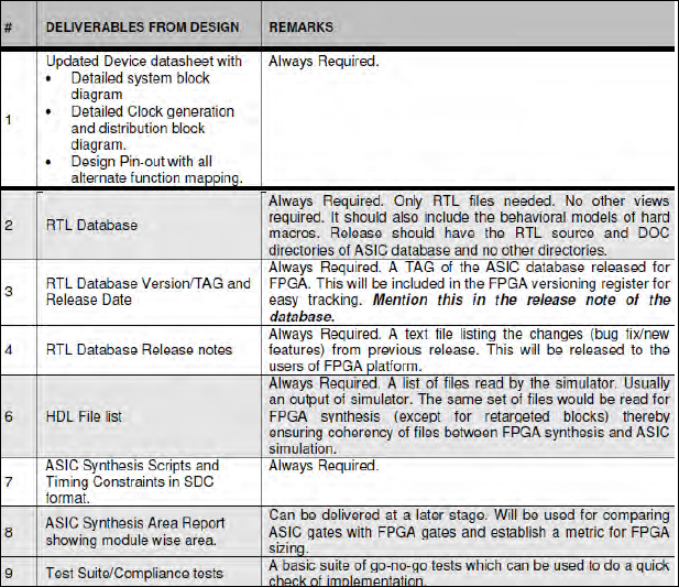
9.2.2. Define list of deliverables for prototyping team
At the start of a prototyping project, the prototyping team needs more than just the RTL. It is important to have a hand-off list of deliverables so that we can check it before the start of the project, or at least understand early on what is missing.. In this way the prototyping team will not waste time later in the project.
Table 23 shows a typical list from a major semiconductor prototyping lab where a design-for-prototyping methodology is being pioneered.
Table 23: Example of design hand-over checklist before prototyping project starts
9.2.2.1. Reuse file-lists and scripts
It may seem like a simple idea but all scripts and file lists should be kept as part of the source control of the project. By capturing more than just the RTL code it will be possible for others to recreate the build process if needed in the future. The best solution is to create common project make-files for SoC and FPGAs with macro-driven branching for different targets. In this way, the design team captures all key details involved in a “run-able specification.” Ideally, most target specific differences will be isolated to independent modules that can be used as a library for a given target. The alternative of laboring to write lengthy instructions may still fail to document all important setup details and discarding key build scripts is asking for trouble later. By just establishing simple procedures and “mindset,” this important chore can become routine activity.
The key point that must be addressed by the team is that a single RTL description will be implemented in two target technologies (FPGA and SoC). A conscious effort should be made to separate technology specifics from the intended functional definition. It is important to create clean architectural interfaces with identical behavior in both implementations. Design practices incorporating this idea during engineering change (EC) activity and quickly communicating design impact in a predictable manner to all team members will increase the effectiveness of the project.
9.2.3. Prototypers work with software team
Some organizations building complex systems with new hardware and embedded software struggle with communication problems between the hardware and software groups. Because of the high software content in a modern SoC, it is critical that the FPGA prototype group regards the software group as its customer. Part of the ROI for the prototype is giving software developers early access to functioning hardware and the two groups must have good working relationship to achieve this goal.
A process to track software changes alongside RTL changes will minimize confusion and wasted effort due to compatibility issues. All changes to RTL code should be tracked by a source code control system (like Perforce or SCCS), probably the same one that is used by the SoC and software developers.
Since the prototype will run slower than the final SoC implementation, some areas of the software may need to be rewritten for error-free operation running on the FPGA prototype. Also the designers of the prototype hardware need to consult with the software developers to consider establishing extra probing points, resets or other capabilities that can help in software debug and which are not possible in the SoC implementation. The important point is that early interaction between the two groups can establish extra requirements on both the software design and the prototype design that will help the project achieve it goals and can be included in schedules at the front-end of the planning cycle.
9.3. Integrate the prototype with the verification plan
The decision to use an FPGA prototype needs to be reflected in all aspects of the chip design project plans. This is particularly important in the verification flow. The project should create branches at RTL maturity points for prototype use. Avoid frequent and incremental RTL dumps on prototype designers. The goals for prototype use in the organization should be clearly stated and reflected in testing plans and project milestones.
Many of the issues concerning planning of the tasks to develop a prototype design are discussed in section 4.2
9.3.1.1. Optimize scheduling of prototype development
The prototype is intended to be a surrogate for the final SoC chip to demonstrate functionality at near-SoC speeds for software developers and others to gain confidence in the correctness of the design. The prototype is not an RTL debug tool – that is the role of the software simulator. We should be careful to wait for the RTL design to reach a pre-agreed level of maturity before starting the prototype development.
There often is a milestone in the design project plan where the team considers the RTL complete enough to issue “hello world” in the simulator. This often coincides with the project milestone when the RTL is ready for a “trial implementation” to identify problem areas in the backend path to silicon. By developing the prototype based on this key RTL milestone will minimize disruption to the prototyping effort from RTL debugging changes and maximize the organization’s use of the prototype.
9.3.1.2. Keep simulation scripts for prototypers to use
As the SoC design and FPGA-based prototype evolve in different directions, we should try to maintain the working simulation models. Then, at key points in prototype bring-up and debug, odd behavior can be checked against working testbenches for the real soC design. Block-level testbenches in particular, are useful for checking RTL modifications and it is best if the SoC verification team shares key testbenches with the prototyping team.
The goal is to leverage everyone’s experience and avoid needless duplication of effort. Identifying a set of “golden” testbenches will build confidence that everyone is working on the same version of the design.
Assuming that the verification team has been busy while the FPGA-based prototype has been developed, there is a chance that they have already expanded their testbench beyond that running when the RTL was delivered for prototype. It is worth having a procedure in house where simulation results are available for inspection by the prototype team or, better still, the verification team can offer insight into faults seen in the prototype. It could be that the same fault has already been detected and possibly even cured in their RTL already. Regular comparison of prototype and SoC simulation results is recommended.
9.3.2. Documentation well and use revision control
Designers should always strive to write clear, self-documenting code. However in any large design there will be some areas where the intended behavior may be subtle and obvious to the creator but not easily understood by others. In these cases, even a few in-line comments around curious design elements will help. This is especially important for late design fixes to avoid wasted effort due to misunderstandings about assumed code behavior.
The larger organization needs to instill the importance of these efforts across all members of the design team so individuals will take the time to use appropriate coding style with comments when first entering the code. Judgment needs to be used to know when simple code can stand on its own and when naturally complex algorithms or unavoidably tricky code will require extra comments to capture the intended behavior for later maintainers of the code.
On top of this, changes that are made by the prototyping team themselves should be recorded in the same revision control system (RCS) as the rest of the project. We should avoid the prototyping team seeming isolated as “those hackers with the boards” about whom nobody has a clear understanding.
9.3.3. Adopt company-wide standard for hardware
As mentioned in chapters 5 and 6, the choice of hardware platform is crucial to ongoing prototype success. If we are looking to do many prototype projects then it will save a lot of time and money to adopt a standard platform. If boards are in stock or readily available from a standard board supplier then inventory issues need not occur, even when boards become damaged and a quick replacement is required.
If boards and add-ons are compatible across multiple labs and sites then a company-wide knowledge base and expertise can be built up around the chosen platforms. Add-on cards might be developed to attach to the standard base platform for a certain project but would then be reusable across the team and wider company.
The worst-case scenario can be that each team obtains or builds a new and incompatible board for every prototyping project, involving risk and high development costs. Further information about this can be found in Appendix B.
9.3.4. Include Design-for-Prototyping in RTL standards
Most RTL style changes for FPGA-based prototyping are also good practices for SoC design in general (e.g., clear functional architecture, FFs at block boundaries, etc.). Specific guidelines should be incorporated in the company RTL coding standards for future projects. Perhaps just enforcing some existing “motherhood” standards is now possible with the requirement to map the generic RTL design into two target technologies so there is less temptation to “cut corners” in design specifications.
As experience with prototypes is gained over time designing similar SoCs, it should be possible to find commonality in the prototypes. Consider creating company standards for prototype hardware to encourage reuse and facilitate common add-on devices.
Although the prototype systems are not usually customer-ready products, they should be built to proper engineering standards as they can serve as a reference design for later work and in some cases become the basis of follow-on product designs. In this way the ROI for the original prototype design may be increased several times over.
Even for the original SoC product, if market opportunity creates the need for a slightly modified product, the existence of a reusable prototype system can greatly accelerate development of the new product and reduce risk in verification of the new functionality.
It is a mistake to think of the prototype as a “throw away” step in the process to get to final silicon of the SoC part. Should a major problem be identified in the field, the prototype can be used again to fully verify the engineering changes (EC) that may have caused it.. Following well-documented conventions and practices will enable subsequent design teams to leverage the earlier prototypes when needed.
Examples of coding standards that will benefit the prototype include naming standards for target-specific design elements (such as clock generation, clocks, memories, and analog blocks), check-in regression and linting requirements, and the careful maintenance and enforcement of a concise coding standard document.
9.4. Design guidelines
So far we have explored how procedure can improve the success rate of FPGA-based prototyping with the various teams. Let’s now summarize more technical recommendations, many gathered from other places in this book but some introduced here in this overview for the first time. The following table, which is split across two pages, summarizes the main technical recommendations for the whole SoC project team to follow in order make FPGA-based prototyping a more productive part of the project.
Table 24: Summary of technical recommendations in Design-for-Prototyping
| Recommendation | Comment/Detail |
| Avoid latches | Latch-based designs allow lower power SoC but are hard to time when mapped into FPGA. |
| Avoid combinatorial loops | Sometimes not seen in SoC RTL because of bottom-up design flow. |
| Pre-empt RTL changes with define | define and ifdef included in source style guide to include/remove prototyping changes. Use single define for all RTL changes. Used to isolate BIST, memory instantiations, etc. |
| Low-impact source changes | Always use wrappers and make changes inside those. Replace files, rather than edit them. Back-annotate changes to real source. |
| Write pure RTL | Allow SoC tool flow to infer clock gating, insert test, apply low-power mitigation etc. avoid instantiating such measures directly into RTL source. |
| Isolate RTL changes | Make changes inside library elements (RAM, IO library etc.) rather than outside of them in the RTL structure. This improves portability, and places the prototyping code close to the original code it is replacing. |
| Reuse file-lists/scripts | Common project make-files for SoC and FPGAs with macro-driven branching for different targets. |
| Memory compatibility | For each new memory generated for SoC, generate FPGA-compatible version. This could be alongside and options controlled with define. |
| PHY compatibility | PHY blocks in SoC will need modeling in FPGA, or in off-chip test chip, if available. Keep this in mind when choosing PHY components for the SoC. |
| Design synchronously | Avoid asynchronous loops, double-edge clocking and other structures which do not map easily to FPGA. |
| Avoid long combinatorial paths Isolate clock sources in own block |
Use pipelining in RTL to break up very long chains of gates which will run much more slowly in FPGA. Keep clock gating and switching in own block, preferably at top level. allows easy and complete replacement by FPGA equivalent. |
| Synchronize resets | Resync reset at each clock domain boundary. Helps avoid race conditions between clocks and reset after partitioning. |
| Simplify clock networks for FPGA | SoC clock networks are very complex. If possible, implement only a subset of full clocking options for prototyping, use define/ifdef to do this. |
| Synchronize block boundaries | FFs at block inputs and outputs add latency but dramatically simplify timing constraints and increase performance |
| Synchronize at clock domain crossings | Generally good practice to use synchronizers. |
| Document any design strangeness | Even a few in-line comments around curious design elements will help. Especially key for late design fix. |
| Keep simulation environment available | During prototype project, odd behavior can be checked against working testbench. Block-level testbench useful for checking modifications. |
| Think at architectural level about slow running design | Allows core and peripherals to run at different rates. Allows deep data buffering between slower running FPGA and external data at full speed. |
| Consider network-on-chip communication vs. wide buses | Industry trend towards “locally synchronous, globally asynchronous” designs will help prototyping. |
9.4.1. Follow modular design principles
Modular design is an architectural approach to design wherein special attention is given to creating simple, reusable, and individually distinct functional units to more effectively address the goals of the project. Modular design can and should be utilized from early in the project specification all the way through design and even in the prototyping flow itself. Good modularity in the original RTL structure will affect the prototyping effort.
One example of a modular approach (which has bearing on the prototyping effort) is the specification and design of multiple modular channels. These could be scaled up or down to more or fewer channels, and enable single-core operation of a multi-core (or mult i-processor) design. Another example is enabling culling of logic that is not conducive to FPGA adaptation, and considering how this might be accomplished in a way that is simple for the prototype designer without interrupting other project goals.
There are almost always test modes, experimental clock modes, and atypical clock modes that are not required by the prototype. Frequently, it is reasonable to remove them using stub files, or by replacing registers with constants, etc., and then allowing synthesis to cull the coupled logic. The implementation in the flow might utilize ifdef’s, libraries, code generators, or constraint files (via RTL modification tools which enable the designer to preserve the purity of the original RTL, but maintain the flexibility to better accommodate the prototyping flow).
The creation of stub files can also be very helpful to the prototyping effort as well as other aspects of the design process when implemented on other functional units. Typically a stub file will consist of whatever interface logic is required to enable the function of the rest of the SoC. In many cases, this may just be a set of constants and pass-through signals to appropriately drive the default values of outputs.
Recommendation: use modular coding style with technology-independent logic elements. Introduce target technology elements only at leaf level or at well-defined functional blocks.
9.4.1.1. Create simple modules
Beyond just using generic logic, it is important to keep the design modules simple and small. Try to avoid making the code excessively general purpose. An RTL design can have excessive complexity when designers attempt to make a module so flexible that it becomes virtually unusable in any specific context. The design of state machines is another example where keeping it simple can be helpful. Some state machine designs span across many pages of case/if statements. This type of design is indecipherable to anyone but the original designer, weak for reuse, prone to error, and difficult to modify. If these machines also include the write-address mechanism for a large register file, it will be very difficult to modify the code in a way that will make the most efficient use of FPGA memory.
Refactoring is another important concept to consider in the SoC design process. Refactoring simplifies code through small redesigns when problems are discovered with the architecture, interfaces, etc. This can include reorganizing functional blocks or dataflow, redefining interfaces or bus protocols, and so on. Refactoring frequently includes extracting common code from one or more blocks and implementing it with more singularity of purpose (often in a single block or function).
9.4.2. Pre-empt RTL changes with ‘define and macros
The RTL code will need to be modified in some areas for the target technology implementations and this needs to be done in a manner to isolate the change while preserving the original structure. A good method to pre-empt prototyping changes is to use define and ifdef macros. Standard macro names could be adopted and these should be listed in the company-wide source style guide along with guidelines for their usage. In that way a single macro definition at the top-level or in synthesis scripts can be used to allow or mask a large number of RTL changes made to the prototype. Example uses of a macro could be for isolating BIST or memory instantiations.
9.4.3. Avoid latches
While latches can be implemented in the FPGA, they can be inefficient and cause complications in timing analysis. For example, latch-based designs can be used to achieve a lower power SoC but will not be correctly processed by the synthesis FPGA technology mapping tools because the power-saving behavior is not fully modeled in the original RTL.
If latches or FFs could be used to the same effect in the SoC then we should try to use FFs instead of latches; it will simplify the adaptation of the RTL for prototyping. One way to accommodate this type of design is to automate the implementation of latches after the synthesis of a gate-level netlist based on FFs. This may be done on the entire chip, or on an as-needed basis for specialized blocks that require latches. In the later case, it may simplify the task if steps are taken to isolate or otherwise mark the sequential elements requiring conversion.
9.4.4. Avoid long combinatorial paths
If the SoC is designed to be used with the latest technology library then it is very possible that there might be 30 or more levels of logic in some combinatorial paths between sequential elements. This may be perfectly permissible in SoC designs where these levels can be placed very close together and have intrinsically low delay in any case. In an FPGA the logic in these paths will be rationalized as much as possible and mapped into look-up tables (LUTs) but nevertheless, some ten or more LUTs may be needed to create the same critical path. The delay of the LUT is not such a problem as that of the interconnect between them, which might be difficult for the place & route tool to keep short, especially if there are many such paths or the FPGA utilization is too high.
If long paths are expected in the SoC design then it would be preferable if these could be broken into sub-paths by the use of pipelining, which would require some rescheduling in the design.
9.4.5. Avoid combinatorial loops
Combinatorial loops can cause unpredictable behavior in general. Intentional loops to create oscillators or state elements should be replaced with black boxes that can be mapped to technology specific implementations later in the flow.
Unintentional loops can result from incomplete RTL, for example, when not all values are specified in case statement or else statements are missing from if trees or even if default conditions are missing inside always blocks. These would all be caught by even the most superficial simulations, but synthesis tools may generate logic with unintended behavior in these situations.
Loops are sometimes not seen in SoC RTL because of bottom-up design flow and the loops are only completed when the whole design is assembled top-down. Potentially, this first top-down assembly may only occur at the start of a prototyping project. (Note that synchronizing block boundaries eliminates this and many other pitfalls.)
The behavior of circuits containing feedback loops is dependent upon propagation delays through gates and interconnections. Due to process variation and temperature effects, such circuits may be unstable in a given technology and should be avoided.
By carefully re-specifying the logic definition to clearly state the desired function will usually eliminate the combinatorial loop.
9.4.6. Provide facility to override FFs with constants
Consider the possibility of overriding registers with constants wherever possible to increase the adaptability of the SoC design. Examples include configuration registers, such as those used for test modes, experimental clock modes, and atypical clock modes.
These can be implemented with ifdef macros, code generators, stub files, or constraint files. The synthesis tool will then propagate the constants-eliminating logic that can cause difficulties in the prototyping flows. This can be useful for ATPG flows that are not based on post processing a gate-level netlist and the elimination of clock muxes tied to unused clock configurations, etc. An approach to constant forcing should be taken which leaves the RTL source intact for later use in SoC implementation.
9.5. Guidelines for isolating target specificity
An important modularity concept is the object-oriented notion of “hiding” extraneous levels of definition details from the usage. Using wrappers and other isolation techniques to locally contain or group design elements will help preserve interesting functional reference points in the prototyping flow.
9.5.1. Write pure RTL code
A disciplined effort should be made to create the full RTL description of the chip in terms of generic logic elements or Synopsys DesignWare® components which are well supported by most FPGA vendors. The SoC designer must avoid calling any low-level primitives directly from the target technology library or introduce an explicit clock in the design. Allow the SoC tool flow to infer clock gating, insert test, apply low-power mitigation, etc. Avoid instantiating such measures directly into RTL source.
Designers generally follow top-down design methods owing to successive refinements for implementation, technology-specific details become entangled into the RTL and it is no longer “pure.” For many design teams, that means modifying the RTL description over time so that the actual RTL passed to the prototyping team contains many low-level technology library primitives intermixed with pure RTL elements. This practice will needlessly complicate an FPGA-based prototype and lead to potential errors.
Recommendation: keep the reference RTL design pure and carefully introduce technology specific details only at the leaf level so alternative FPGA and SoC definitions can co-exist in the design database.
By maintaining a pure RTL description of the design it will be possible to isolate all target technology specific details. This is essential to allow sharing of the base RTL code while providing supplemental detail for the FPGA implementation and the SoC implementation separately.
9.5.2. Make source changes as low-impact as possible
Once the generic RTL design has been established, further changes should be done locally without introducing new modularity. Always use wrappers and make changes inside those design elements. Replace files, rather than edit them. Back-annotate changes to real source files.
Make changes inside library elements (RAM, IO library etc.) rather than outside of them in the RTL structure. This improves portability, and places the prototyping code close to the original code it is replacing.
9.5.3. Maintain memory compatibility
Specialized elements or “cores” with optimized implementations are used in FPGAs for bulk memories. It follows that each memory element in the RTL design must be assigned alternative technology specific definitions for FPGA and SoC mapping. This approach will result in the most efficient use of chip resources and insures that some thought will be given to proper modeling of each memory element. For each new memory generated for SoC, just supply a FPGA-compatible version using vendor technology macros. The necessary code for each technology could be side-by-side in the RTL source file and the selection between options controlled with define.
For the most part, synthesis tools are familiar with the target technology and can map RTL code into FPGA elements in a process known as inference. Whenever possible, having RTL synthesizable behavioral models will improve the FPGA adaptability of our code. There are examples of the use of wrappers and synthesizable memories in chapter 7.
This approach relies on technology mapping algorithms in the synthesis inference tool, however a better implementation may be possible using the library or manual design-file replacement mechanism. One way to do this would be to create a special target direct (perhaps with “_fpga” or a similar prefix) and keep files of the same name as those they are replacing in that directory. With some tools, you can add this list to the end of a current file list, and they will thereby override the original RTL higher in the file list. With others, you may need to create a second file list. There are scripts available from Synopsys that help automate the file list management. This flow should maintain as high a level of target isolation as possible, and avoid having any miscellaneous logic not unique to the SoC/FPGA border.
9.5.4. Isolation of RAM and other macros
It is good practice to introduce an enclosing block or “wrapper” around every technology-dependent element of the design. This includes configured RAMs and other specialized macros in the technology library, which are not generally available in other technologies. Wrappers are allowed break rules about only having logic on lowest levels of RTL as they create a well-defined unit which is replaced with functionally equivalent logic in the SoC design.
The process of including such elements is as follows:
- Create the FPGA element using the tools supplied by the FPGA vendor (such as the Xilinx® CORE Generator™ tool, Memory Interface Generator, etc.). Typically we specify the core type, the target technology, defines the various parameters’ initial-states values, etc.
- The FPGA tool generates the desired core’s FPGA netlist and initialization file, where applicable.
- The netlists are used in the place & route stage, and the template file is used to instantiate the generated core into the main design.
- In addition, the tool generates a wrapper file containing functional simulation customization data that, combined with the primitive model used in the core, can be used for functional simulation.
- Add RTL code to instantiate the template file in the design, and connect the module to the design.
Recommendation: use optimized FPGA macros and RAMs to improve FPGA resource utilization and speed, enclosing technology dependent code within a wrapper block to facilitate substitution of SoC implementation and creation of functional test point for verification.
9.5.4.1. Note: handling RAM in formal verification
As we approach the issue of how to implement SoC RAMs in the prototype, we should also address the question of “how do I verify that the behavior of my FPGA RAMs are equivalent to my SoC RAMs?”
Also, the prototype builder should be considering how to verify equivalency through the entire process of converting the SoC design to FPGAs. Doing so will save time later.
The process of using formal verification (FV) on the designs would be much easier if equivalency checking were considered early in the prototyping phase. If we can plan for FV from the beginning with a methodology for verifying the RAMs using testbenches and then plan to formally verify the remainder of the design by black boxing the RAMs, then FV can be a more useful tool. This should be consistent with the use of FV in a general SoC design methodology.
9.5.5. Use only IP that has an FPGA version or test chip
While FPGAs are the main prototyping resource in a typical prototyping system, some SoCs may have a few blocks that either do not map into FPGAs, or blocks for which better prototyping resources are available. Such blocks are typically analog circuits, or fixed digital IP blocks for which neither source code nor FPGA netlist is available. In these cases, we will need to consider solutions outside the FPGA to model the block in the prototype.
IP suppliers typically provide evaluation boards with the IP implemented in fixed silicon. In other cases, the prototyping team may design and build boards that are functionally equivalent to the IP blocks that do not map well into FPGA technology. In still other cases, existing or legacy SoCs may be available on boards as part of the prototyping project and can be added to and augment the FPGA platform.
By using separate hard IP resources for these blocks we will benefit from higher performance (compared to FPGA implementation) and will use less of the FPGA’s resources..
Recommendation: use plug-in hard IP “evaluation” devices on the prototype board when available to improve prototype speed and reduce complexity of FPGA logic.
9.5.5.1. Note: PHY compatibility
Embedded IP blocks in the SoC that are provided from the vendor as a physical block without detail RTL description will require special coding in the RTL. If a test chip is available for the IP it should be connected to the prototype board as an external plug-in and the RTL written to use this off-chip connection. Otherwise the IP will need to be modeled with a generic RTL functional definition of the algorithm to be mapped to the FPGA. Keep this in mind when choosing PHY components for the SoC and planning overall architecture of the FPGA prototype. For more information about IP in FPGA-based prototyping see chapter 10.
9.6. Clocking and architectural guidelines
The complexity of today’s SoC designs require specific attention be given to overall RTL design architecture related to clocking and managing major synchronous blocks in the system. FPGA technologies are more constrained in the available resources for managing multiple clock domains than custom SoC technology. There will typically be multiple FPGA parts needed to fully model the SoC design, imposing some board-level clocking requirements. Our goal is to abstract some notion of a global clock architecture that can be shared in the RTL description between both the FPGA and SoC implementations. The following guidelines will help manage this complexity.
9.6.1. Keep clock logic in its own top-level block
If the clock generation logic is kept independent of the rest of the design, it will be more adaptable. Likewise, we should strive to keep unrelated or loosely related design logic out of the clock generation block. Moreover, the independent functional aspects of the clock generation should also be separated into easily recognizable modules. Frequently, there are many more options in the clock-generation logic than are required for the FPGA or even for SoC for that matter. If a block is well separated from other unrelated logic, the block can be replaced by a prototype-specific block that simply drives a few clocks at constant frequencies.
In many cases we may be importing IP with its own internal clocking structure. There may be some value in hard-coding (or at least optionally hard coding) clock selection logic, or otherwise simplifying the clock modules in the IP, if the complexity is no longer required for the specific use model. It may even be possible to completely remove certain components of the clock-generation logic and thereby greatly simplify one of the most involved tasks associated with prototyping.
Keep clock gating and switching in their own blocks, preferably at the top level. This will allow easy and complete replacement by FPGA-equivalent structures.
9.6.2. Simplify clock networks for FPGA
SoC clock networks are often very complex. In general, an SoC has much greater clock flexibility than does an FPGA. If possible, implement only a subset of the full clocking options for prototyping, Use define/ifdef to control RTL expansion while retaining the full complexity for SoC synthesis.
Simplifying the clock structure is key to the adaptability of the design. Even if your SoC clock structure is thoroughly documented, it may be difficult to implement in the FPGA if it’s extremely complicated. One of the biggest contributors to clocking complexity is test logic. Often automatic test pattern generation (ATPG) circuitry inserts logic to multiplex clocks. Note that an FPGA, being reprogrammable, ships fully tested. There is almost never a reason to include ATPG logic in the FPGA prototype. Including it introduces unnecessary complexity to the FPGA clocking structure. If the insertion is automated it can easily be disabled for the FPGA implementation.
However, some test logic may be required in the FPGA prototype. For example, almost all microprocessor designs include some sort of serial debug interface that works through a JTAG clock. This is absolutely necessary for doing software development on the FPGA. It is helpful to partition the test logic into that which is necessary for only the SoC and that which is necessary for the FPGA. At a minimum include comments in the code to indicate which is which. Also indicate in the comments how signals should be tied off to disable test logic that’s unnecessary for the FPGA. Ideally, insert “ifdef FPGA … else … endif” pre-processor commands to separate functionality required for the FPGA prototype from that required for the SoC. In the “ifdef FPGA” clause, tie off unnecessary test logic inputs to their disabled values so that this logic is pruned in FPGA synthesis.
9.6.3. Design synchronously
Avoid asynchronous loops, double-edge clocking and other structures that do not map easily to FPGA. Limit the overall design to conventional synchronous design methods. If unusual structures are required in the SoC design then isolate those circuits to local blocks, which can be replaced with equivalent functions in the FPGA design.
Maximizing the use of conventional synchronous design style will greatly simplify the effort required to develop the FPGA prototype.
Minimize the portions of the design running on clocks required for external interfaces, and use asynchronous FIFOs whenever possible to transfer data to and from these interfaces to the system clock domain.
9.6.4. Synchronize resets
Remember that the FPGA configuration process initializes every block RAM, distributed RAM, SRL, and FF to a defined state even if no reset is specified in RTL, so explicit code is not required as it is in the SoC. Depending on how the resets and presets are defined, they can have a significant impact on what can be inferred and therefore how much of the FPGA’s special resources can be automatically used. The key point is to spend more time earlier considering the reset strategy, and write the reset logic in a way that is simple, consistent, and flexible. If some of these FPGA considerations can be accommodated it will enable many creative solutions.
9.6.5. Synchronize block boundaries
Use FFs at all block inputs and outputs. This practice will add latency and require rescheduling of modified paths with respect to the rest of the design, but it dramatically helps to apply timing constraints and to meet timing targets. It also assists in chip layout and FPGA partitioning. Certainly we should already be synchronizing at clock domain crossings.
Often it is not practical to modify the design scheduling specifically for the FPGA. However, if the common design practice of inserting FFs at the boundaries of each designer’s block is observed, the likelihood of having FFs between partitions is substantially higher. If we follow the practice of synchronizing boundaries then we should have far fewer exceptions to handle when it comes to constraining the FPGA prototype.
9.6.6. Think how the design might run if clocked slowly
Prototypes are constructed from multiple FPGAs, a printed circuit board, custom IP core plug-ins, and other components. The design architecture of this mixed-technology solution must allow the cores and peripherals to run at different rates. Thought must be given to the interfaces between all of the elements and whether we need to provide deep data buffering between slower running FPGAs and external data that is running at full speed.
If addressed at the architectural level, the expected speed differences between SoC and prototype implementations can be cleanly isolated and managed properly. For example, in many cases rate adapters are required for the FPGA prototype. Often, if considered early in the architectural phases of the design, major functional modules’ bus interfaces can be designed such that speed bridges are not required. Because of the independence afforded by this architectural style, resultant designs tend to be more robust, adaptable, and readable as well.
9.6.7. Enable bottom-up design flows
The ability to easily implement a bottom-up design flow can be very advantageous to the implementation of the prototype. Many of the design and architectural recommendations already mentioned will naturally enable bottom-up design flows. (The concepts of synchronicity, simplicity, and isolation all typically provide benefits to these flows.) We can enhance bottom-up flows further by considering how synthesis tools create automated enhancements.
If high-level modules are kept free of parameters and generics, a bottom-up flow will require less effort from the tools or engineers attempting to pre-process and uniquify the modules.
An exception to the preference of keeping clock logic in its own top-level block may also be considered to more easily enable clock conversion in bottom-up flows. If gated-clock conversion is being implemented, we may want to consider moving the final on/off gating to the module which is being selectively disabled, so that this type of conversion can be automatically handled by the synthesis tool without error-prone manual hierarchical modifications.
9.7. Summary
The main point of our Design-for-Prototyping manifesto is that the use of FPGA prototype reshapes the development task by providing a confidence-building “executable specification” which, through its speed and RTL clarity, empowers the individual groups within the design team to work more effectively to achieve the SoC design project goal.
The key proposals of Design-for-Prototyping are:
- Development of FPGA prototype is a key element in the overall SoC design project and so needs to be included in plans and schedules.
- The RTL design needs to follow a robust coding style to effectively represent both FPGA and SoC technologies, both in first coding and ongoing refinements. The resulting quality of RTL definition will pay dividends throughout the life of the design.
- Use modular coding styles including clean separation of prototype-specific components from the rest of the design, independent dataflow, and isolation of clock do mains.
- Expand design documentation to identify as early as possible challenging parts of the design to the prototyping team.
- The SoC Team might need to realign slightly in order to integrate prototyping in their processes and staff skill sets to maximize the possible benefit.
The end result of these seemingly obvious but perhaps arduous changes will be that FPGA-based prototyping benefits will be derived earlier in the project, enabling earlier software validation and pre-silicon integration.
The authors gratefully acknowledge significant contribution to this chapter from
Mark Nadon of Synopsys, Austin