CHAPTER 12 |
BREAKING OUT OF |
There are situations in which taking a prototyping system outside the development lab can benefit the development and the overall success of the product. Having a portable prototyping system can provide developers with the ability to interact with other parts of the system not available in the lab, and showcase the product before silicon is available. This chapter describes the issues and effort that it takes to make a hardware prototyping system portable, so it can be used outside the R&D lab as well .
12.1. The uses and benefits of a portable prototype
The hardware prototyping system is usually considered very close the final SoC as far as its functionality and performance, however, its form-factor is often so far from the final SoC package that it isn’t even funny. Try as we might to keep things tidy and regular, a typical on-the-bench prototype often looks like the result of barely controlled chaos … but it only looks that way.
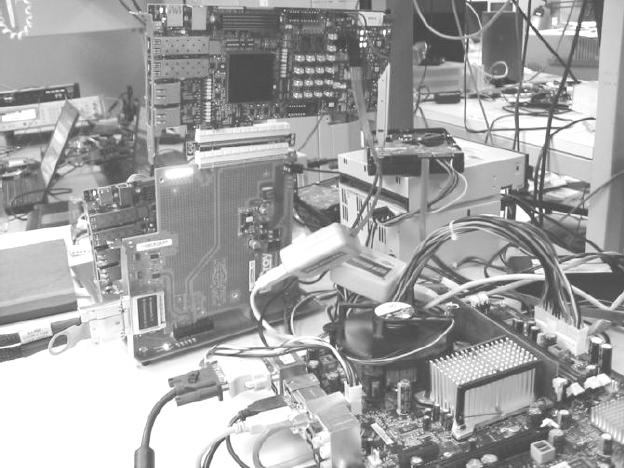
As we assemble our rig on the bench, such as the typical one shown in Figure 147, we of course know exactly why each piece of equipment is present and how it contributes to the overall success of the project. In fact, the project shown in the photo is a Synopsys® lab test of our latest PCIe Gen3 IP design, which at time of writing was proceeding very well and providing unique feedback on the performance of the IP as only an FPGA-based prototype can.
What if the prototype could be constructed small and robust enough so that we could take it to out of the lab? What extra benefits, which may prove critical to the overall success of the SoC project, could be derived?
Figure 147: A typical bench-bound prototype!
Before we proceed to explore how we might achieve portability, let us revisit those benefits of prototyping that we listed in chapter 2 in order to highlight the main reasons why we might want to take our prototype out of the lab.
- Field tests: our application may have functions which require field tests under real-world conditions that are not available in the lab. A good example is a mobile radio transceiver which needs to communicate with a base station under many and varied ambient conditions.
- Local compliance tests: wireless standards evolve at different speeds and may have variations for different geographies. For compliance we often require that air interface tests are performed in that geography.
- Early customer demo: a portable prototyping system at a potential customer site can show off the product’s capabilities and readiness for market.
- Partner co-development: early pre-silicon access to the system prototype enables product development and test that spans multiple geographies, often involving a number of companies in partnership.
- Exhibition demo: being first to demonstrate a new functionality or new standard implementation can gain great momentum in a market..
- Investor status check: a portable prototyping system can be used to demonstrate a product’s capabilities to a board of directors or potential investors alike. Our audience can quickly and effectively evaluate our progress when presented with a live demo of the final product’s prototype.
Each of the above may be good reasons for any particular team creating a more portable prototype than the bench-bound example above. In fact, the Synopsys IP team responsible for that prototype did package it up for demonstration out of the lab. Torrey Lewis, IP developer at Synopsys, Hillsboro Oregon, explains why they did that extra work:
“It is definitely a benefit to be able to travel with the prototype. For our PCIe Gen3 setup, we’ve been able to travel to some conferences for display in the Synopsys booth. The PCIe Gen3 spec is not yet finalized, so even more interesting for me as an engineer has been the opportunity to do early testing on-site with industry leaders. This has been mutually beneficial for all concerned.”
Let us now go on to see how we can make a prototype which is able to break its bonds to the bench.
12.2. Planning for portability
The best time to plan for portability is when we start our prototyping project. It is best to plan for prototyping system portability at the project start and make provisio ns for it as the system and the SoC is developed. For example, if we are aiming at a multi-board system comprising one main board with additional daughter boards then we must ensure that our arrangement can be made robust when necessary.
Javier Jimenez of DS2 also feels that reliability is important in their out-of-lab trials of their Broadband-over-Powerline prototypes, as he explains below:
“Some of our field trials are performed by engineers from different disciplines, for example, protocol experts or software engineers. These are not hardware experts and so they could not be expected to perform on-the-spot fixes to circumvent any board failures. Therefore the FPGA boards, and indeed the whole prototype must be of high quality and have high mechanical reliability.”
You can read more about DS2’s project in chapter 2. Meanwhile, the following sections explore the critical items for building a prototyping system that is portable.
12.2.1. Main board physical stiffness
The obvious first concern is that the board itself should have inherent stiffness and not flex in out-of-lab situations. The main board should be stiff enough as to not flex either lengthways or crossways. Since today’s FPGAs are most useful for prototyping in ball-grid array packages, the strength and quality of the FPGAs solder-ball connections to the motherboards is critical to the overall system reliability. Little or no flexing of the board can be tolerated unless these ball connections are broken.
Typical prototyping boards with multiple high-pin count FPGAs will end up having over 20 layers and become fairly stiff on their own. However, it is still recommended to make space for stiffeners in both board’s length and width so that they may be mounted when necessary. Alternatively, the board might be slipped into a frame which hold the board at its edges, however, this is not as mechanically sound as on-board mounted stiffeners.
12.2.2. Daughter board mounting
Daughter boards are added to the main board for a variety of reasons such as adding fixed hardware to the FPGA system. When these boards are designed to work with the main FPGA board, we must consider the mechanical, electrical and thermal aspect of the combined assembly as described in the following paragraphs:
- Stacked configuration: in this configuration, the daughter board is mounted over the main board and its footprint overlaps the main boards. The advantage of such configuration is the smaller overall footprint. The disadvantages are the possibility of restricted probing access on the main board and the risk of restricted air flow over the FPGAs. Both main and daughter boards must be designed for solid mounting of the two.
- Lateral configuration: in this configuration, the daughter board is mounted next to the main board. This is typically the case when the daughter board is not designed in house, rather purchased or provided by a third-party IP vendor and its mechanical configuration is unrelated to the main board. The advantage of such configuration is having unrestricted access on the main board. The disadvantage is the greater overall footprint and tendency to be less robust.
12.2.3. Board mounting holes
Main board should have sufficient mounting holes to allow a secure and solid mounting to a chassis. It is recommended provide for mounting holes no more than
10cm apart from each other in either direction. Special attention should be paid to areas where the board is subjected to connector insertions. It is recommended to place mounting holes such that the mounting studs will absorb most of the connector’s insertion and extraction forces that are typically perpendicular to the board. If additional daughter boards are to be added on top the main board, there should be allowance for mounting the daughter boards to the main board. This is discussed in more detail in the section below.
12.2.4. Main board connectors
Connectors are often a common point of failure in the prototyping system’s reliability due to wear and improper mount and dismount cycles in a typical lab environment. Addressing the connectors’ issues in advance can minimize this risk especially when we need to move the combined system. Connectors are typically made to mate with either in only one axis, so twisting or skewed removal or insertion may cause damage. We recommend adding adequate strain relief and retention in the insertion-removal axis; in fact, many connector schemes have an option for such retention clips already and it is a false economy not to install these by default.
Cables that exit the system’s enclosure must be retained to the system’s chassis rather than rely on the retention by the connector itself, which adds further strain onto the connectors and cables alike.
12.2.5. Enclosure
The enclosure is where all the pieces fit together for convenient transportation but at the same time some level of access and visibility is needed. When selecting an enclosure, the following items are typically considered:
- Mechanical configuration: even if the system is intended to be placed on the bench, many of the shelf enclosures are available in industry standard sizes so they can also be mounted into a standard rack. The additional rack mounting hardware can easily be removed if found to be undesired.
- Main board mounting: it should be mounted with as many screws/spaces as available.
- Daughter boards: as mentioned above, should be secured either to the main board (if stacked) or to the chassis with no mechanical stress between the daughter board and main board.
- Power supply: should be placed away from the main board to allow good clearance for main board cabling and cooling for the power supply. If the system is expected to travel to countries where AC is different than the country of origin, the power supply must be multi-voltage. If power supply has its own exhaust fan, it’s important to mount it to the chassis in a way that does not obstruct the cold air inflow to the power supply module.
- Internal cables: should be retained on the boards they mount to.
- External cables: should also be retained to the chassis.
- Access: Most access to the system is done via the system’s interface cables. However, some provision may be needed for debugging, so critical signals may be brought to debug connectors for added visibility. These debug connectors should be mounted on the chassis wall so opening the chassis will be not necessary.
- Miscellaneous items such as FPGA download module, or debugger modules should also be retained to the chassis.
12.2.6. Cooling
When in the bench, the FPGAs and other components are generally exposed to ambient airflow and may not require extra cooling. However, even on the bench, it is recommended that each FPGA should have its own heat sink and fan arrangement. This can be linked to a temperature system monitor in a feedback loop to ensure that the fans are only used when necessary (see chapter 5).
Even if on the bench we do not employ any cooling, when the prototype is encased and isolated from ambient air movements, the temperature can rise rapidly. It is recommended to equip the enclosure with cooling fans that will draw hot air from the enclosure and blow it to the outside. The key to effective cooling is the positioning the enclosure fan and cold air intake such that cold air is drawn from the intake holes and forced over the hot spots and out the enclosure via the enclosure fan. This is usually accomplished when the exhaust fan and the cold air intake holes are on opposite sides of the enclosure. It’s recommended to block any openings that may be next to the enclosure fan so as to not “short circuit” the air flow over the “hot spots.” It is still necessary to provide local heat-sinks and fans for the system’s hot spots, such as FPGAs or power supply circuits.
12.2.7. Look and feel
For some out-of-lab uses, it is important that the prototype looks less like a school science project and more like a finished product. This can be achieved by, in effect, hiding away much of the hardware inside a professional looking case. This has the added bonus of making the prototype more tamper-proof and probably more reliable as a result.
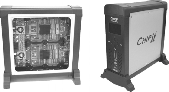
Some commercial FPGA platforms are designed to be more robust and portable than a typical open board. Examples of this type of system are the CHIPit® Platinum and CHIPit Iridium platforms, both of which have sophisticated FPGA boards encased in robust enclosures. The Iridium, shown in Figure 148, is a particularly interesting example because it is clearly still a prototyping platform, you can see the boards and chips in place, but by replacing the sides on the enclosure, the unit becomes much more like a finished product. This simple trick may count for a lot in a demonstration scenario.
Figure 148: CHIPit® Iridium, an encased prototyping system
The best places to go and see how teams overcome the portability challenges are so-called “plug-fest” events. These are organized by special interest groups, often representing a new industry interconnection or graphics standards. The aim is to bring together those teams which have hardware for driving the new standard so that they cam physically plug their equipment together. Of course, all teams would have already been working to the standard specifications but there is nothing like the confidence given when the pre-silicon prototype actually works with another team’s prototype. Even if it doesn’t work straight away, this is a much better place to find out than after the product is released.
Critical to the success of plug-fests is the reliability of the equipment and even though much of it is in FPGA-based prototype form, we will see platforms carried between table-top lab set-ups or moved around on trolleys in order to perform as many experiments as possible. Turning up at a plug-fest with a “rats nest” of unreliable boards would not be making best use of the opportunity.
12.2.8. Summary
This has been a short chapter exploring the use of FPGA-based prototypes outside of the normal lab environment. It has hopefully given some more glimpses of the possibilities of prototyping as a whole, but the aim is really to ensure that we think ahead to create a more reliable and portable prototype. This will make it more tamper proof when used remotely by, say, software engineers and more likely that the prototype will survive the project and be useable for subsequent projects.
The out-of-lab use of prototypes can often be decided upon well into the project, for example at an exhibiton opportunity that it just too good to miss, but the first silicon is still months away. Being ready for these kinds of events may be recognised by senior management as another reason to adopt FPGA-based prototyping in all SoC projects.