CHAPTER 13 |
PROTOTYPING + |
Having decided to invest in building an FPGA-based prototype, we should understand its full potential. This chapter shows how the prototype can become a part of a larger verification environment by linking it to simulators, emulators or virtual models in SystemC™. In other sections of this book we have focused on how to create FPGA prototypes. This chapter looks at how design teams benefit from integrating their prototypes into hybrid verification systems. We also look at the enabling technologies for hybrid verification solutions, including the verification interfaces themselves.
13.1. System prototypes
System prototypes are hybrid verification solutions that incorporate elements of hardware (including FPGA-based systems), software (virtual) models, and traditional EDA simulators. Bringing these technologies together enables designers to mix and match modeling solutions to get the best out of their resources, and to meet their design and verification needs.
There are two core technologies that underpin most system prototyping solutions and enable them to communicate. Co-simulation typically brings together RTL simulation and hardware at the cycle level. The simulator and hardware work in lock-step and communicate through signal-level links. Design teams use transaction-based communication to connect virtual models and hardware using abstracted messaging.
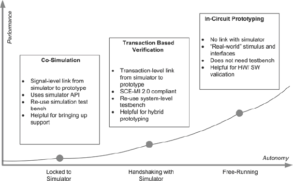
Figure 149 compares co-simulation, transaction-based verification and in-circuit prototyping in terms of relative performance and autonomy. Linking the prototype to a simulator allows the testbench to control the hardware, but at the expense of reduced performance compared with the free-running prototype.
Figure 149 Comparing three approaches to linking FPGA prototypes
13.2. Required effort
Unfortunately, we cannot just plug a prototype into a simulator and expect it to work. Getting a hybrid verification system to work is not always a push-button exercise, although tool environments will automatically generate some of the code that is needed. On top of having code for interfaces, designers have to perform some design conditioning to enable co-simulation and transaction-based verification.
If a design team knows that it will use its prototype in a hybrid verification environment before we start to implement it, the incremental effort required is not that great. It’s difficult to quantify the extra design work needed because it depends on many variables. Preparing a design for co-simulation is a question of setting a few constraints within the tool environment. The effort required to enable a design for transaction-based verification depends on whether transactors are already available or need to be created. It is probably reasonable to add 10% to 15% to the “time to prototype” effort in order to ready the FPGA for transaction-based verification.
In order to decide whether the incremental effort is worth it, designers need to know what they can achieve with a hybrid verification environment.
13.3. Hybrid verification scenarios
There are several use scenarios for hybrid verification. We have checked that the scenarios mentioned here are real, not hypothetical. Synopsys engineers have talked to many design teams about their prototyping plans, and this is what they are already doing, or planning to do in upcoming projects.
Design teams often have pre-existing RTL from legacy projects, or have acquired RTL IP for parts of their systems. Reusing existing RTL and targeting it to an FPGA prototype, then combining the FPGA prototype with a virtual model, enables design teams to quickly create a full system model.
Using a pre-existing virtual model for a complex processor core, while using FPGAs to model peripherals, enables design teams to accommodate complex processors and have them run faster than if they were implemented in an equivalent FPGA model.
Somet imes, design teams start out with a virtual model of the whole system. As RTL becomes available or matures, they can replace parts of the virtual model with the new RTL and re-run the tests. If runtimes are short, the design team will re-test the RTL using a normal simulator. Otherwise they will use the hardware.
Using FPGAs with daughter cards or plug-in boards enables the hybrid model to access real-world IO. For certain repetitive tasks it may be beneficial to replace real IO with virtual IO – for example, when it is important to replicate exact inputs for regression tests. This removes any uncertainty to do with using real-world data, since it guarantees an absolute repeat of previous stimulus conditions.
By keeping the FPGA prototype remote and providing software developers with access via their desktops, they can have all the benefits of access to real-world IO, but within a familiar development environment (i.e., keyboard and screen).
For many design teams, the benefits of some or all of these use modes make the investment in enabling their FPGA prototypes for hybrid verification more than worthwhile. We will look again at each of these scenarios in more detail later in this chapter.
13.4. Verification interfaces
To enable the use scenarios outlined above, we need to interface the various parts of a hybrid verification solution and bring together simulators, physical hardware and virtual models. We shall now explore some of those interfaces.
13.4.1. Interfaces for co-simulation
To enable co-simulation, we need to provide a cycle-accurate bi-directional link between a high-performance RTL simulator and an FPGA-based prototyping system
Ideally, we want the link between the technologies to be easy to set up and require no changes to the design itself. Performance of the interface is important, and ideally the link will offer good debug features.
To avoid confusion, it is worth comparing the use of FPGA hardware linked to simulators and a similar technology, known as “hardware in the loop” or HIL. HIL replaces a block in a simulation model with a faster piece of hardware, usually implemented in an FPGA. The aim is to use the FPGA to speed up simulation of the algorithmic model. The FPGA is programmed with some automatically generated code, which is often only functionally equivalent to the simulation model that it replaces and will not be cycle-accurate. The initial design in an HIL approach is often an algorithm modeled in a simulation tool, such as Matlab® or Simulink® and there is no reference to the RTL that will be used in the SoC implementation.
In contrast to HIL, the aim of linking FPGA-based prototyping to simulation is to use the same RTL as the SoC implementation in order to check the validity of the FPGA implementation, possibly with some speed-up of runtime, or to allow system-wide prototyping before the whole RTL is available.
13.4.1.1. Example: HDL Bridge
It is useful to look at an actual co-simulation interface by way of example. HDL Bridge is Synopsys’ proprietary co-simulation link. It provides a bi-directional interface between Synopsys’ RTL simulator (VCS®), and the FPGA-based prototyping system (Synopsys CHIPit® or HAPS® prototyping system). The CHIPit tool can automatically prepare the infrastructure to communicate between the simulator and hardware based on the RTL provided by the user. CHIPit creates wrappers without disturbing the original design – a synthesizable wrapper for the hardware (either Verilog or VHDL) and a separate wrapper for the software simulator.
This environment is easy to set up and allows seamless integration with VCS simulation. Once constrained, generating the wrappers is very fast as we need only provide the top-level design description, define the clock and reset polarity.
The interface enables comprehensive debug by allowing the simulator to monitor all internal registers of the design under test (DUT) in the FPGA.
Figure 150 shows how the HDL Bridge is partitioned so that the non-synthesizable part of the interface remains in the simulator, while the synthesizable code is implemented in hardware. The wrappers get data from the hardware and software and give it to the simulator’s PLI interface as it makes PLI calls. The simulator testbench controls the design.
Figure 150: HDL Bridge co-simulation partitioning
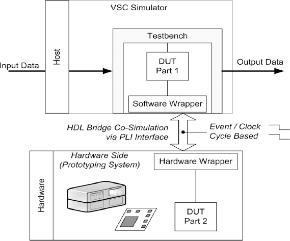
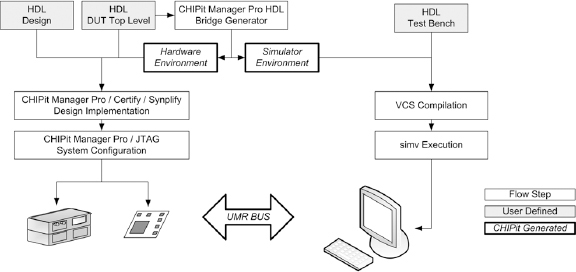
Figure 151 shows the overall design flow for the Synopsys environment and highlights the user-defined inputs and the automatically generated code.
Co-simulation suffers from a fundamental limitation: because the simulator is only capable of running at a speed of a few kilohertz, and the hardware runs in lock-step, it is not possible to use real-time interfaces or components that have a minimum frequency such as technology-dependent primitives including PLLs, DCMs and IP PHYs. We have covered the issue of addressing FPGA minimum frequency in chapters 7 and 9, which readers should consult for recommended design strategies.
Figure 151 HDL Bridge co-simulation design flow
Recommendation: design teams can save themselves time by thinking ahead and anticipating issues. Planning the clock structure to support a low-frequency clock will make the task of setting up for co-simulation easier
Another issue that designers must watch out for is the trade-off between debug and performance. HDL Bridge allows designers to monitor the internal registers in the FPGA, as they increase the number of signals to monitor, the performance of the interface decreases.
In summary, co-simulation can take advantage of any simulator’s API in order to push stimulus to the hardware and receive its responses. It is easy to set up and no design changes are necessary. The tool takes care of preparing the infrastructure to communicate between the simulator and hardware once we have created a top-level description and defined the clock and reset signals.
13.4.2. Interfaces for transaction-based verification
In co-simulation, the simulator is controlling the design in hardware, while in transaction-based verification, the DUT (in hardware) and simulator (or software application running on a host machine) communicate by passing messages or transactions. This requires an abstracted bi-directional link between virtual models and the FPGA-based prototyping system.
Communicating through transactions and the use of transaction-level models enable faster simulation and easier debugging than co-simulation. Using transactions, design teams can focus on the function and behavior of their systems and get that right before they concern themselves with implementation. They can also define the verification scenarios that they want to cover more quickly and easily, because they are using software running on the processor.
13.4.3. TLMs and transactors
The SystemC transaction-level modeling standard (TLM-2.0) defines two coding styles: loosely timed (LT) and approximately timed (AT). TLM-2.0 models, which themselves include transactors, enable efficient message-based communication for exploring the system at a high level of abstraction when written in an LT coding style. A model that includes an LT transactor is relatively fast to develop because the transactor simply deals with reads and writes to memory locations.
However, in the hardware world we cannot ignore timing forever. That is why TLM-2.0 allows designers to create transactors with timing annotations by writing models using AT coding styles. Using these, design teams can perform tasks such as estimating software performance and analyzing different architectures. Developers can create AT models relatively quickly.
As designers refine their systems down to real hardware, they need to add even more timing detail. To enable this we need transactors that can convert from the function level to and from the signal level. For example, taking TLM-2.0 transactions to, for instance, AMBA® AHB/APB/AXI™ interconnect signals, and also handling side-band signals such as reset inputs and interrupt request outputs. These transactors have a cycle-accurate interface to RTL on one side, and a transaction-level interface on the other side.
Design teams can achieve high-speed transaction-based verification by processing the compute-intensive part of the transactor in hardware, rather than using software on the host workstation. This is possible if the transactor is coded as a synthesizable state machine, or bus functional model (BFM), which receives messages and converts them into signals that are connected to the design ports or internal buses. Developing transactors for complex interfaces such as AXI can be time-consuming, so reuse is extremely desirable.
The transaction-level interface between the synthesized and simulated parts of the design is made up of fixed-width unidirectional input and output ports. An input port sends messages carrying transaction-level information from the simulated testbench layers to the hardware-assisted layer. An output port sends messages from the hardware-assisted layer to the simulated layers. There can be any number of input and output ports. However, the hardware platform may place some restrictions on their number, width or total width.
13.4.4. SCE-MI
The Accellera standards organization approved version 2.0 of the Standard Co-Emulation Modeling Interface (SCE-MI) in 2007. SCE-MI provides a multi-channel message-passing environment for transaction-based verification. The standard defines how messages can be sent between software and hardware.
SCE-MI enables design teams to link transaction-level models to hardware accelerators, emulators and rapid prototyping platforms by interconnecting untimed software models to structural hardware transactor and DUT models (Figure 152). It provides a transport infrastructure between the emulator and host workstation sides of each channel, which interconnects transactor models in an emulator to C/C++/SystemC (untimed or RTL) models on a workstation.
Figure 152 High-level view of runtime components in SCE-MI based co-modeling
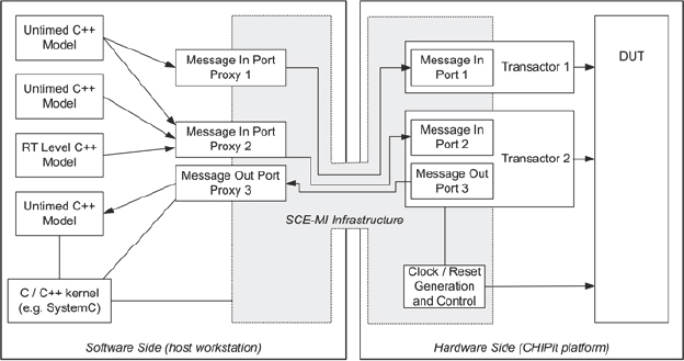
In SCE-MI version 1.1, the transport infrastructure provides interconnections in the form of message channels that run between the software side and the hardware side of the SCE-MI infrastructure. Each message channel has two ends. The end on the software side is called a message port proxy, which is a C++ object that gives API access to the channel. The end on the hardware side is a message port macro, which is instantiated inside a transactor and connected to other components in the transactor.
A message channel is unidirectional – either an input or an output channel with respect to the hardware side. However, a message channel is not a unidirectional or bidirectional bus in the sense of hardware signals, but resembles a network socket that uses a message-passing protocol. The transactors are responsible for translating the message-passing protocol into a cycle-based protocol at the DUT interface. They decompose messages arriving on input channels from the software side into sequences of cycle-accurate events which can be clocked into the DUT. In the opposite direction of informationfl ow, transactors recompose sequences of events coming from the DUT back into messages to be sent via output channels to the software side.
Furthermore, the SCE-MI 1.1 infrastructure provides clock (and reset) generation and shared-clock control using handshake signals with the transactors. This way the transactors can freeze controlled time (by suspending the clocks) while performing message composition and decomposit ion operations.
SCE-MI 2.0 adopts SystemVerilog’s direct programming interface (DPI) function-call model and adds additional features to enable transfer of bi-directional variable-length data between the DUT and the software testbench using just four functions and pipes.
Table 31: SCE-MI 2.0 hardware and software calls
| Hardware call (h/w to s/w) | Software call (s/w to h/w) | |
| Data transfer | Import function | Export function |
| Streamed data transfer | Send pipe | Receive pipe |
In case of SCE-MI 2.0, the clock delivered to the SCE-MI transactors is controlled by the infrastructure and therefore user intervention is not required to stop and start these clock signals.
Recommendation: if there is a huge amount of data to be sent, then it is necessary to use pipes. We can use data transfer functions if there are only control signals or small amounts of data to be sent. If data transfer functions are used for large amounts of data the handshake overhead can exceed the size of the packet sent.
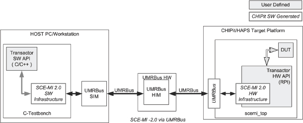
13.4.5. SCE-MI 2.0 implementation example
In this example, illustrated in Figure 153, the transactor and infrastructure communicates with hardware through the UMRBus®. Synopsys’ CHIPit tool uses the user-defined transactor description to create the hardware infrastructure for the DUT, and also writes out C/C++ files for the software environments. The communication between software and hardware uses its own clock domain (SCE-MI clock), which is independent of the DUT’s clock domain. During data transfer between the host software application and hardware via SCE-MI, the SCE-MI controlled clocks are stopped on the hardware. SCE-MI infrastructure releases the controlled clocks once the data transfer is complete. Users do not need to take any special steps to manage this – the control clock handling procedure is part of the SCE-MI 2.0 infrastructure.
Figure 153: SCE-MI 2.0 co-emulation overview for CHIPit®/HAPS®
Another way to use SCE-MI is to communicate with a simulator incorporating SystemVerilog testbenches. The SCE-MI 2.0 standard defines a way to communicate between software and hardware. If users need to communicate with a simulator within a SCE-MI 2.0 environment, Figure 154 shows how the simulator’s SystemVerilog testbench can talk via SystemVerilog’s DPI calls to a C-environment, and the very same C software can talk to the connected hardware via DPI-like SCE-MI 2.0 function calls.
Figure 154: SCE-MI communication through DPI
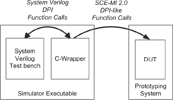
Figure 154 shows, on the right, a hardware system with a SCE-MI DPI function. The simulator executable (left) includes a C-wrapper file which has SCE-MI DPI functions, as well as a pure SystemVerilog communication channel that enables communication between the C software and the SystemVerilog testbench. The VMM hardware abstraction layer (VMM HAL), which is described below, is an example of this approach.
13.4.6. VMM HAL
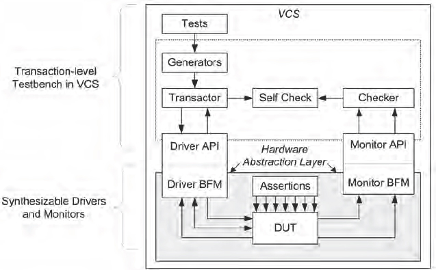
The Verification Methodology Manual (VMM) defines a methodology for verification that has become widely adopted by design teams. The VMM HAL is a VMM application that includes a class library to support transaction-level co-emulation between a hardware-accelerated design and a VMM-compliant testbench running on a SystemVerilog simulator, such as Synopsys’ VCS functional verification simulator.
The hardware abstraction layer enables designers to use different hardware acceleration platforms with the same constrained-random testbench that is used in simulation-only environments. Testcases and DUT can target different hardware platforms without any modifications. Figure 155 gives a very brief overview of the VMM approach and we see that there is a verification loop driven by high-level, often object-oriented code which hardly resembles a testbench in the traditional sense. The loop would normally continue via transaction-level drivers into the DUT and out through transaction-level monitors to complete the loop with some comparisons and a scoreboard of results passed.
With the HAL, the transaction-level drivers and monitors are replaced with SCE-MI2.0 transactors and the DUT is the FPGA-based prototype containing a version of the SoC design.
The VMM HAL application also contains a purely simulated implementation of the hardware abstraction layer that allows the testbench and testcases to be developed and debugged with the DUT entirely within the same simulation, without modifications, and without access to the hardware emulator.
Figure 155 HAL-compliant transaction-level testbench
The VMM HAL environment can target hardware or simulation at runtime by using a simple simulator command-line switch. The environment includes drivers and monitors, which are software-software transactors in a normal VMM environment. VMM HAL transactors for hardware must be synthesizable.
Some companies are starting to build up VMM HAL transactor libraries. A key benefit of the VMM HAL is that it maximizes reuse of testbench code. A designer does not need to modify the top layers of the verification environment (such as tests, generators and transactors), only the lower-layer monitors and drivers need to be made HAL-compliant.
13.4.7. Physical interfaces for co-verification
Physical interfaces for co-verification are those implemented in the prototyping environment to support communication between a host system and hardware. The physical layer can use any transport mechanism, and design teams can opt to use a standard PC interface like PCIe. Whatever physical interface they settle on, ideally it should offer ease of use for faster validation of the hardware prototype, better design debugging and easy prototype configuration. Support for advanced use modes will also be beneficial, especially support of: standard APIs; RTL-based co-simulation and debugging; accelerated transaction-based verification; and connecting to and co-simulating with virtual prototypes. Interfaces that enable rapid initialization of the system and remote access and management of the FPGA-based prototype allow design teams to get the most use from their prototypes.
Synopsys has designed the UMRBus physical interface specifically to provide high-performance, low-latency communications between a host and Synopsys’ FPGA-based prototype platforms. We previously introduced UMRBus in chapter 11 in the context of debugging. To recap, UMRBus is a high-speed connection between the host workstation and the prototype that provides parallel access to all FPGAs, board-level control infrastructure and memories (internal and external) on the Synopsys FPGA-based prototyping platforms.
13.5. Comparing verification interface technologies
In order to compare different verification interfaces, Synopsys has created a demonstration benchmark based on an image processing sub-system. The demonstration system uses a JPEG algorithm to compress an image, which is stored on a host computer. We first simulated the RTL in VCS running on the host computer before moving the DUT from simulation to a synthesized target running on an FPGA prototype, which enabled us to compare co-simulation with HDL Bridge, SCE-MI and UMRBus.
The comparisons and performance data are summarized in Table 34 later but in the meantime, Table 32 summarizes the comparison between the four different modeling techniques.
Table 32: Summary of performance and benefits of four interface implementations
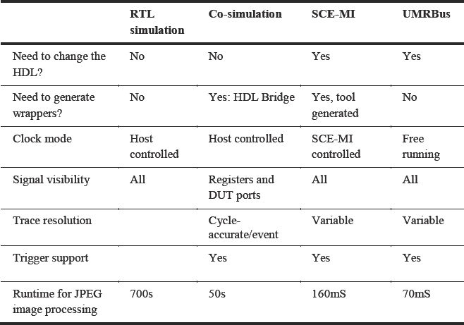
For this particular task, we can see that UMRBus is the fastest implementation. SCE-MI, implemented on top of UMRBus is second fastest thanks to its use of transaction-based communication. Co-simulation using cycle-based interfaces for this task is about 300x slower than SCE-MI, and RTL simulation is over 4000x slower than SCE-MI. While this data helps us to compare the different approaches, it is not possible to generalize. Performance depends on many different parameters, for example, how much computation is happening on hardware and how much is in the simulator, also, what is the amount of data that is being exchanged between different sides of the transactors, and what transport mechanism is used? Of course we will also get different results for different kinds of design.
The UMRBus channel is for the sole use of the co-simulation and SCE-MI implementations. Using an alternative bus standard, such as PCIe, may deliver worse performance as the channel is not a dedicated interface and it may have to handle other traffic as well as the co-simulation data.
As well as considering performance, it is worth comparing the debug capabilities of each approach. UMRBus enables users to interact directly with the design from the software world. Intensive debug activity in HDL Bridge or SCE-MI may reduce overall performance. The number of signals that we can capture in HDL Bridge may be limited.
It is also possible to perform debug by physically connecting to the FPGA using a logic analyzer and physical probes. This allows probing of internal FPGA signals, and it is useful for tracing free-running designs. There are a couple of potential drawbacks with this approach to debugging – there may be a delay on debug traces, and probe signal names may not exactly match the original RTL names.
13.6. Use models – more detail
Having gained a better understanding of the types of interfaces available for co-simulation and transaction-based verification, we look in more detail at the use models we summarized earlier in this chapter.
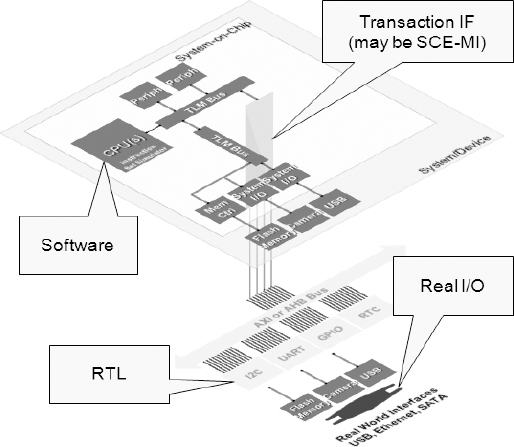
13.6.1. Virtual platform re-using existing RTL
In this case (Figure 156) the project team wants to use a virtual platform, although they are concerned about the overall modeling effort required. Because they need good performance, they decide to instantiate the RTL in the FPGA rather than a simulator. It may be that they are developing a new architecture, so they want to start to develop software before all the RTL is available.
In this case we can provide a virtual platform with, for instance, the latest ARM® core, which will probably be available before ARM has actually introduced it as RTL or physical IP. The core could be modeled in the virtual platform but we may need to integrate it with a high-performance sub-system for which we do not have a system-level model. For example, that might be a high-definition video codec for an imaging sub-system for which we have RTL code from a previous design. We can decide to implement the codec in the FPGA, gaining accuracy and performance, but keep the rest of the design in the virtual prototype, at least until that RTL also becomes available.
It might take two to three months to bring up a new prototype from fresh RTL but to create a virtual platform model from scratch might take even longer but it would still be quicker than waiting for the new RTL. By mixing virtual models and legacy RTL we can have a better chance of bringing up a hybrid system in the quickest time. The other benefit of a hybrid system is that at least part of the design will have cycle accuracy.
Figure 156: Virtual platform re-using existing RTL
13.7. Virtual platform for software
FPGAs are not optimized for processor implementation, so a design team that wants to use a complex processor, such as an ARM Cortex®-A8 or similar, will find it difficult to instantiate the core in the FPGA and achieve the performance they are looking for.
One option (Figure 157) is to partition the design so that they have a fast ISS running within the virtual platform. They have to partition the design sensibly so that they can perform most of the transactions in software, and only when accessing peripherals should the system access the FPGA. They should ensure that all the local memory (e.g., L3 memory) is also within the virtual platform; otherwise they would see no performance benefit as a result of going across the SCE-MI interface to fetch instructions and data.
Figure 157: Embedded software executed on host
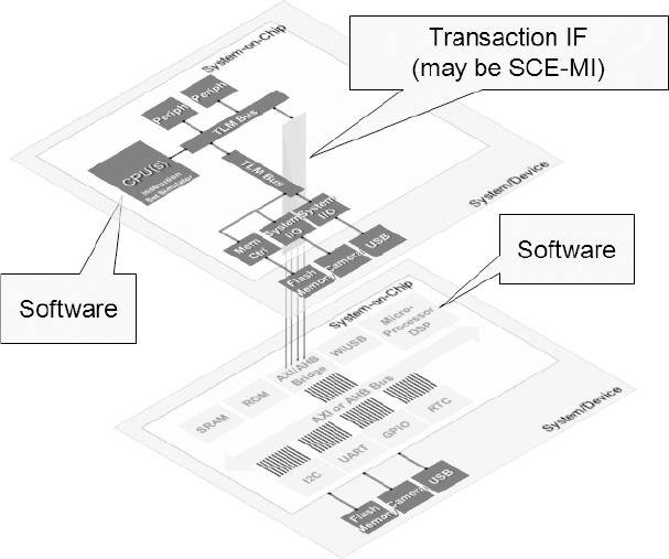
In this example the design team performs native execution of the embedded software on the host PC. Executing software on a workstation with a virtual model processor is often faster than in FPGA prototype. The design team can use the FPGA to maintain the accuracy of accelerators and peripherals.
13.7.1. Virtual platform as a testbench
Design teams tend to use this approach (Figure 158) when they have kicked off the project with some pre-RTL software development. They may have actually started to write test cases to verify some of the blocks in the virtual platform. This is an approach that we have used within Synopsys to verify USB software.
When the RTL becomes available, they can replace the TLMs with the RTL instantiated in the FPGA and re-run the same software verification tests against the RTL to check that they pass, or otherwise refine the test cases. While some of the IP blocks that they have modeled may have only partial functionality, they will have full accuracy (including the introduction of cycle-accurate timing) in the RTL. By abstracting some of the accuracy at the outset, the developers can get started on the software development sooner.
Figure 158: Virtual platform acts as a testbench for RTL in FPGA

Using the virtual platform as a testbench for the FPGA prototype avoids duplication of effort by making better use of the work that went into system-level development. It also enables a design team to compare results in simulation against results in hardware, to verify the flow into hardware by repeating a set of known stimuli, to provide feedback to the verification plan for quality assurance purposes and to run regression tests very efficiently.
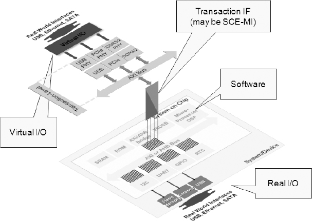
13.7.2. Virtual and physical IO (system IO)
In this scenario (Figure 159) the design team has a certain amount of virtual real-world IO that it can support from the virtual platform, but this situation is not as good as having a real physical interface. To reduce risk, we need to verify the design in the context of the system it lives in, by connecting it to the real world. Any new interface standard would benefit from this approach.
Design teams want to implement standards before silicon is available. We can support this requirement by using a plug-in board (physical hardware) that would confer the ability to use a standard virtual platform to bring up an OS, like Linux. In this case we would have a new IP block and would be able to interface it to the real world for test purposes.
Take the example of integrating a camera in a phone applications processor chip. Taking this approach we could link the baseband design to a camera on a workstation and make the software believe that information is coming from the real camera in the phone. This allows the use of real-world stimuli when appropriate.
For some applications it may be useful to create a GUI or some other interface to allow the design team to interact more naturally with the virtual environment. For example, “Can the phone receive a call while playing a game and downloading email?” is the kind of scenario that using a GUI will help to verify.
Figure 159: Virtual platform with a physical connection to the real world
13.7.3. Virtual ICE
Sometimes software developers do not want or need to see a board on their desks, yet they do need access to the functionality that the DUT provides in order to write code. This approach (Figure 160) provides a virtual hardware capability and helps to keep software engineers out of the lab and in the comfort of their familiar development environment – at a PC.
With a virtual ICE the design team can give remote access to the software developers – virtual ICE is the remote desktop solution. They can have a very small element of a virtual platform running on each of the software developer’s desktops.
The idea is that the design team has an FPGA model that includes interfaces like LCD and UART. They direct those interfaces back up to a virtual platform on a PC so that they can have an LCD instantiated on the user’s desktop. They would redirect the hardware traffic back across SCE-MI, giving a software virtual interface to the hardware. Rather than connecting the FPGA to a physical LCD or physical UART, they would model those interfaces within the virtual platform. They implement the majority of the system in FPGAs, and provide virtual interfaces to some of the physical hardware ports.
Figure 160: Platform provides links to designers at their desks
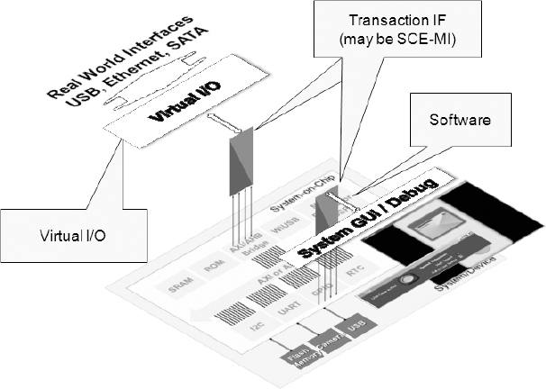
This approach is especially beneficial if the prototype has to remain in the lab because of its size or fragility. The disadvantage is that simulation performance will be worse over the network than having a high-speed connection direct to the prototype.
13.8. System partitioning
Getting the hardware-software partition in the right place is critical to achieving good system performance. There are a number of issues that designers must consider, as well as some practical guidance to follow.
First, there are certain fixed constraints. Some parts of the system – for example, the testbench – may just not be synthesizable, so the design team cannot place them in hardware. They may also be constrained by design size and need to map the design to multiple FPGAs. Remember that high utilization of the available gates leads to longer implementation times, especially because of place & route.
For parts where they have choice, design teams need to decide where to put the bridge between hardware and software. They can only make a cut where they can use a transactor that already exists, or that they can easily obtain. This tends to favor inserting the partition at well-defined industry standards, such as on an AHB™ bus interface. Making a cut at some arbitrary point means that the design team has to come up with a way of modeling it, which can create problems.
Once they have considered the constraints, the design team must analyze the design to understand where they can make the cut in order to reduce the communication between the simulator and the hardware. To maximize the chances of having the FPGA accelerate the design, ideally they need to have computation in the hardware dominate communication between the simulator and hardware.
Whether a design team will see their design accelerated depends predominantly on the traffic across the interface between hardware and software. If the traffic is characterized by a few control signals, the design team will likely see a huge speedup. On the other hand, heavy interaction between the simulator and DUT may yield a small speed-up, or none at all. Table 33 shows how applying Amdahl’s law helps to predict simulation acceleration.
Recommendation: if the aim is simulation acceleration, consider where computation is happening. Move more and more components into the DUT, if possible synthesize the testbench so that everything runs in the DUT.
Table 33: Ahmdahl’s law predicts simulation acceleration
| Share of simulation effort | ||
| Testbench | 90% | 10% |
| DUT | 10% | 90% |
| Maximum acceleration factor | 10% | 900% |
Sometimes, design teams choose to successively refine their partitions by moving more and more into the DUT, as the RTL becomes mature. Not committing untested code to the FPGA helps them to manage risk. For maximum performance they can move across all synthesizable parts of the testbench.
Recommendation: if the DUT uses multiple FPGAs, dedicating the simulator interface to just one of the FPGAs will help improve performance.
13.9. Case study: USB OTG
This case study shows how Synopsys combined a virtual platform and FPGA prototype to create a system prototype for a USB on-the-go (OTG) core.
13.9.1. USB OTG System overview
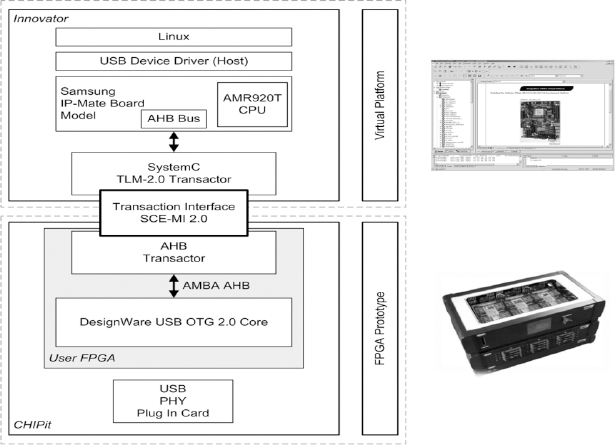
The system (
Figure 161) consists of a virtual platform modeling a Samsung system-on-chip supporting LCD, touchscreen, DMA, and physical Ethernet, running an unmodified hardware Linux image. The virtual platform connects via an AHB bus with transactors over the SCE-MI 2.0 interface to the USB 2.0 OTG core running in the FPGA prototype.
We can connect a USB memory stick containing pictures to the system prototype by using a daughter card. The virtual platform controls the memory stick which provides access to the images. Users can debug at the hardware-software interface with the software debugger and the hardware debug environment.
Figure 161: CHIPit Innovator system prototype
13.9.2. Integration use models
The system prototype enables various use models. One of the key benefits is achieving a significant speed-up over pure RTL simulation – in this case by a factor of 6x. The debug insight and controllability at the hardware-software interface also boosts productivity. The environment supports features such as hardware break-pointing, including the ability to pause and single-step the entire simulation. System visibility and logging is only constrained by the host PC memory and storage capacities.
13.9.3. Innovator and VCS
We can integrate the Innovator model with VCS through SystemC by using PLI TLMs. We can partition the system so that the USB OTG RTL description runs within VCS. The disadvantage of this configuration is that VCS cannot physically control the memory stick. However, we can work around this by reflecting the accesses back up to the software (the virtual prototype), and then connecting to the USB stick.
Figure 162: Innovator and VCS
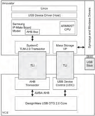
In practice, because the RTL is running much slower than the FPGA it is very difficult to control a physical memory stick. That is why most design teams would choose to use an FPGA prototype rather than co-simulation. There are, however, advantages of using a VCS solution, including its superior analysis capabilities and having better insight into the behavior of the core running on VCS – more so than a designer would have with CHIPit, for instance.
13.9.4. Innovator and CHIPit or HAPS
This use case (
Figure 163) consists of Innovator connected to CHIPIt or HAPS via SCE-MI.
On the software side is a library that allows us to send transactions (which may just be reads or writes) across SCE-MI. In the physical prototype we have a synthesizable transactor that we have implemented in an FPGA, which can then interact with the RTL for the USB OTG.
Figure 163: Innovator and CHIPit (or HAPS)
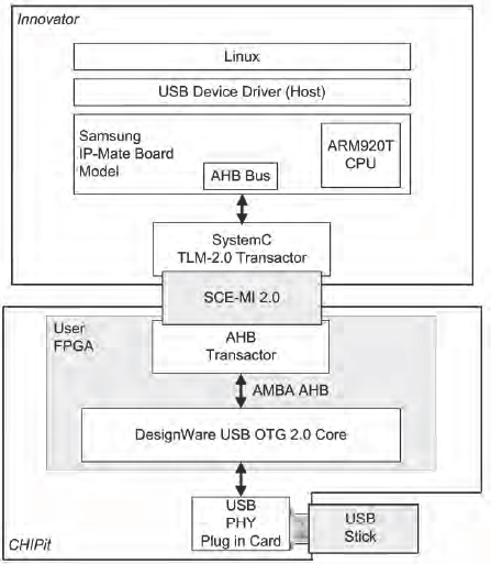
The advantage of having the transactor instantiated on CHIPit is that we can have a plug-in card for the physical USB interface, so we can control a physical memory stick or some other physical real-world device. Because the function is in hardware, it is fast enough to do that. In some cases, this may also differentiate this use case from the pure virtual prototype use case.
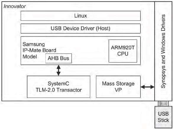
13.9.5. Virtual platform
The advantage of the pure software virtual prototype is that at the pre-RTL development stage, there may not be any RTL available, so there is no other easy way to do co-simulation or transaction-based verification. That is basically why software virtual prototyping complements the hybrid or hardware approaches: developers can start to develop their software, pre-RTL, on a software virtual prototype assuming that they have access to models. It will take a certain amount of time to develop new IP blocks. Despite that, typically we can have customers engaged in software development some 9-18 months before tape-out.
Figure 164: Pure software virtual platform
Performance Comparison Table 34 shows performance figures for booting the system and for performing the mount, copy and unmount operations.
Table 34: Summary performance and characteristics for USB OTG example
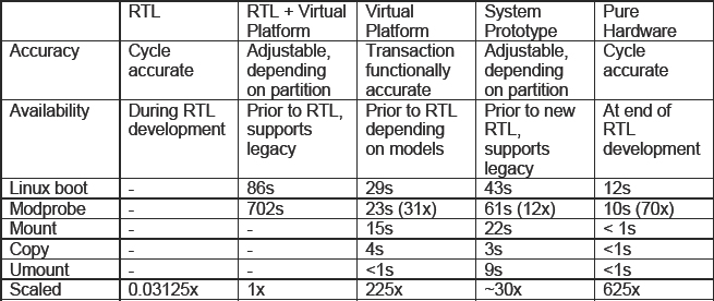
The pure virtual platform performance was actually faster than the system prototype because in this particular design there was a lot of traffic going across from the virtual prototype to the RTL, in order to process interrupts. USB is not the best example to demonstrate performance acceleration via hardware because of the number of interrupts that the core generates and the processor needs to service. In fact, the USB generates a start-of-frame interrupt in high-speed mode every eighth of a millisecond.
We had to look at ways of optimizing this design to stop the interrupts swamping the bandwidth, with the consequence of a decline in performance. We did quite a lot of work to boost the performance of the virtual platform. Partitioned properly, something like a video codec would see better performance with the system prototype than with the virtual platform.
The authors gratefully acknowledge significant contribution to this chapter from
Rajkumar Methuku of Synopsys, Erfurt, Germany
Kevin Smart of Synopsys, Livingstone, Scotland