CHAPTER 15 |
CONCLUSIONS |
We have come to that point that occurs in every book; the end. With a technical book, such as the FPMM, we also need to summarize the lessons learned in the book and reach some conclusions. In this very short chapter we shall endeavor to capture the essence of the previous 400 pages in a short take-away form.
15.1. The FPMM approach to FPGA-based prototyping
Table 35 gives a summary of the various steps and main considerations in running an FPGA-based prototyping project.
Table 35: Summary of steps in FPGA project
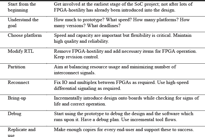
We have addressed each of these steps throughout the chapters of this book and taken one step at a time, and using external pre-made sources as often as possible, we can quickly gather the expertise and tools required to create a successful prototype. Let’s reconsider our three laws of prototyping as reprised in Table 36.
Table 36: The three “laws” of prototyping revisited
| Law 1: | SoCs are larger than FPGAs |
| Law 2: | SoCs are faster than FPGAs |
| Law 3: | SoC designs are FPGA-hostile |
Considering each law in turn, we can summarize the main FPMM conclusions that we found in each case.
15.2. SoCs are larger than FPGAs
Despite, or perhaps because of, 25 years of progress, the first law of prototyping is still pertinent. It is true that many FPGA-based prototyping projects require only one FPGA and this is usually true for IP block verification and in-lab feasibility projects. However, SoC projects are by their nature large and getting larger and while FPGA devices are at the leading edge of silicon development and also getting larger year-on-year, we will probably still need multiple of the largest FPGA devices to prototype a full SoC.
This means partitioning of the SoC design into multiple FPGAs for which we recommend using specialist EDA tools. These will allow us to partition interactively or automatically, the former giving the better results but taking longer.
The typical size of a prototype is between one and ten devices but with sophisticated automated partitioning and programmable interconnectivity, prototypes up to 20 devices are possible. As each device is already just over four million ASIC gates, this represents a design up to 80 or 90 million SoC gates which is way above the size of the majority of SoC designs today.
When the SoC design is partitioned over multiple FPGAs, we will need to perform some extra design work in order to maintain the design connectivity, the clock networks, and the reset and start–up synchronization. These are all explained in chapter 8.
15.3. SoCs are faster than FPGAs
The second law is true when comparing the core speed of both types of device, where the fine-grained and infinitely versatile architecture of an SoC customer chip means that it can outpace an FPGA, with its coarse-grained programmable architecture. So we should expect the RTL from an SoC design with a core speed of many hundreds of megahertz to run in an FPGA with core speeds in the region of 20MHz to 100MHz.
However, this speed is reduced if the design’s critical path crosses the FPGA boundary and especially if multiplexing is used between the FPGAs. Both of these situations are common so the typical performance of a prototype in most cases is between 10MHz and 25MHz. Nevertheless, this prototype speed represents by far the fastest pre-silicon platform possible for exercising the RTL of an SoC design.
So the core speed of an FPGA is relatively fast but the first law holds true. At the IO the FPGA is just as fast as the SoC silicon in most regards and is able to support very much the same standardized peripheral interfaces as the SoC. Indeed, the ability of the FPGA IO to reproduce fast peripheral interfaces is one of their most valuable advantages over slower verification technologies. In addition we can use external PHY devices as well as those built into the FPGA.
All this means that it is common to find FPGA-based prototypes USB at 125MHz, or HD video running at full 72MHz rates. For the IO, therefore, with care and the right IP, we can break the second law of prototyping even if it still holds true for the core logic.
15.4. SoCs designs are FPGA-hostile
After reading chapter 7 we might be forgiven to think that FPGA-based prototyping involves quite a few changes to the SoC RTL but that does not always need to be the case. That chapter covered many possible scenarios and it would be a pathological design indeed that needs all of them to be fixed but, nevertheless, a good prototyping team will not be daunted by even the most FPGA-hostile SoC design. Armed with the best tools, IP, boards and devices and most importantly the right expertise and approach, we can tackle any SoC design and create an FPGA-ready version of at least the majority subset of the design.
However, that is only the minimum acceptable result of a FPGA-based prototyping project and far more is achievable. As we outlined in chapter 9, a Design-for-Prototyping approach will ensure that the SoC design does not arrive as FPGA-hostile in the first place.
We do not have to accept the third law of prototyping as a simple fact of life. A Design-for-Prototyping approach means that we can break the third law and make our SoC designs, if not FPGA-friendly, then at least FPGA-tolerant!
15.5. Design-for-Prototyping beats the three laws
Design-for-Prototyping guidelines fall into two groups; procedural guidelines and design guidelines.
We summarize the procedural guidelines in Table 37 and the design guidelines are not repeated here but instead are included in full in chapter 9.
It is hard to imagine that we will be fully successful if we only follow one set of the guidelines, however. If we had to choose just one, then it is the procedural guidelines that are probably the more important set.
Table 37: Summary of procedural recommendations in Design-for-Prototyping
| Recommendation | Comment |
| Integrate RTL team and prototypers. | Same tool training. Shared knowledge of FPGA and SoC |
| Prototypers must work closely with software team. | Software team are the prototypers best “customer” |
| Include prototype in the verification plan. | Branch RTL at pre-agreed milestones of maturity |
| Keep prototype-compatible simulation environment. | To compare results with original SoC simulations |
| Keep combined documentation and revision control. | Track software and RTL changes for prototype |
| Adopt company-wide standard for hardware and add-ons. | Avoids waste and encourages re-use |
| Include Design-for-Prototyping in RTL coding standards. | Design-for-Prototyping RTL style is also good for SoC. |
The secret of success in many prototyping projects is in this integration of the prototypers with the rest of the SoC design team. This must lead to the inclusion of the prototypers’ needs and their feedback at the early stages of the SoC project. Then, with only small changes to procedure and design style, the success of FPGA- based prototyping can be guaranteed. In return, the software and RTL parts of the SoC are introduced at the earliest possible opportunity with minimum effort, addressing the critical development effort of most SoC projects today, the embedded software.
15.6. So, what did we learn?
The main lesson might be to tackle complexity one step at a time but make sure that each step is in the right direction and not into a dead end. When starting an FPGA-based prototyping project, our success will come from a combination of preparation and effort; the more we have of the former, the less we should need of the latter.
Having read through most of this book, we will enjoy a significant head start to our prototyping projects. We hope that our methodical approach to FPGA-based prototyping will allow anybody to tackle the complexity of their next SoC project with more confidence and achieve even more successful results.