
Introduction
to High-Density Programmable Design
By Lee Hansen, Xilinx Software
Product Marketing Manager, EEdesign
Dec 22, 2000 (9:13 AM)
URL: http://www.eedesign.com/story/OEG20001222S0012
Part 1 of
4
Programmable logic is about to evolve into a new role in the electronic
system. Since the advent of the FPGA over 15 years ago, the number of gates
available on a single device is greater than ever before. The portable device
market is exploding with a vast array of functions previously unimagined.
Complex peripherals are now commonly required to fit into a size no larger than
a PCMCIA slot. Advanced broadband redundant switches today fit into a one-width
rack unit and operate at 3GHz and higher data transfer rates. And while meeting
these demands, the product must still hit the market window faster than ever
before. The consequence to the designer: more functions, packed into smaller
spaces, operating faster, and designed quicker. These time to market pressures
are driving FPGAs to deliver more design solutions and offer more available
complexity.
If you're a digital designer that keeps up to date, you already know this.
But exactly what does this mean to the way you've come to design? Or if you're a
design manager, how will you control this looming environment to your advantage?
If any of the above comes close to describing your company, you're about to
launch into the world of high-density programmable design. This article is the
first of a four part series introducing high-density programmable design, what
defines it, what makes it unique, what differentiates if from other logic design
methods. We'll spend time looking at software design developments that help ease
the transition to high-density design, and get your products out the door faster
than ever before possible. We'll follow a typical design process from creation,
through capture and source options, synthesis and implementation, to chip
verification both during design, and finally when the FPGA is in the system.
Platform FPGA
In November, Xilinx announced the Platform FPGA
initiative, recognizing that FPGAs have matured beyond the original glue-logic
function of programmable logic. With Platform FPGA, programmable devices can now
be the central driving point of the primary board functions.
The Xilinx Virtex-II architecture will push the definition of "high-density",
by packing more functionality, I/O choices, clock management, and memory into
our programmable devices. It? easy to define "high-density" by gate count and
available memory alone; but to the designer "high-density" design is primarily
defined by what those possibilities do to the design process.
Low-Density vs. High-Density
Low-density logic design is typically
about delivering a small set of logic functions, often only one. The FPGA or
CPLD is used to provide an ancillary but vital function of the overall board. If
IP is used, it's usually a combination of math processes or simple to moderate
functions, and used in a limited way. And importantly, low-density designs often
can be completed by a single engineer.
The needs that drive customers to high-density design dictate that the
function of the chip on the board has now changed. In high-density design the
FPGA has now become the heart of the system providing multiple functions, key
bus management, processing, and interface tasks. IP is likely to be used in the
design, and is further likely to drive the critical processes (PCI-bus
controller, DSP functions, etc...). IP becomes a way of solving critical design
problems quickly. Most importantly, only the most masochistic engineer would
want to complete a high-density design alone. Team design moves from being an
interesting concept, to a critical success factor in order to bring a
high-density device to successful delivery.
Start by partitioning
Partitioning the device by functionality is
our starting point, making the design process much more manageable. We start by
dividing the design into hierarchical modules. Many factors will dictate how
these modules should be defined: division points of the available designers;
where can prior design work be utilized; how many functions can be realized
through core or purchased IP blocks; which areas of the design will require
unique or intensive design work and re-work? Most importantly, partitioning the
design correctly can accelerate timing closure by keeping critical gates and
paths together, and also minimizing the number of interface ports between
modules.
Figure 1 shows an example of a device being partitioned using Xilinx
High-Level Floorplanner. The hierarchical modules are now constrained to
specific physical areas of the device. In the process the design manager can
also map I/O if known, or reserve I/O blocks for future use. Floorplanning up
front serves two main purposes. The first is to break a large device down to
manageable sub-designs. Out of floorplanning, the design manager can create
black-box definitions to define the HDL modules. This allows each designer to
receive the correct design definitions of their respective module, while the
design manager can still perform analysis functions at any time from the top
block of the device without requiring all the modules to be complete.
The second is to map those modules onto the actual chip for fitting, as shown
in Figure 1. As each designer works on only one module of the design, completion
is now about finishing logic design and reaching timing closure for that module
only. The full range of design functions can be utilized on any level of the
device, from the top, on down to any given module. And once timing closure is
reached, the timing for that module remains "locked" while the remaining work is
still being completed. Future articles in this series will go into the
importance of this breakdown to Incremental Design, and how the design team can
now see vast improvements on implementation times.
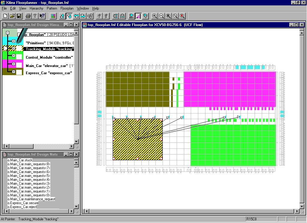 Figure 1 -
Xilinx Floorplanner Figure 1 -
Xilinx Floorplanner
Next Month
Now we?e ready to begin the actual logic design work.
We have a high-density device partitioned into manageable modules for design
capture. Those modules reflect the different design sources we'll be using:
purchased or core IP, reusable design, or custom HDL code. Next month we?l talk
about design capture and IP options, and getting logic design done and ready for
implementation.
For More Information
The xilinx.com website contains more
information on the FPGA Platform Initiative, Xilinx High-Level Floorplanner and
Modular Design; and also the Xilinx Foundation ISE and Alliance family of
software design products.
Copyright 2002 © CMP
Media, LLC
|