The best way to learn
floorplanning?
Just do it
I can't say that I've seen any literature on the art of floorplanning.
Unfortunately really good floorplanning is more of an art than a science. That
should not discourage the neophyte however, as even basic floorplanning can have
dramatic results. The goal is of course to place the logic in ways that make the
routing easier, less congested and shorter. As a starting point, you might let
the tool do the place and route. After it is finished, read the placed design
into the floorplan tool and start looking for ways you can improve the layout.
The first thing you will probably notice is how awful the automatic placers
really are.
For Xilinx designs you will have to get a hold of XACT6. There is a beta
floorplanner for M1.4, but it is really not ready for prime time yet. In my
opinion, there is not enough info supplied with the beta floorplanner for
someone who is not already familiar with the xact6 floorplanner to use it.
Anyway, get a copy of xact 6 and look at the on-line documentation for the
floorplanner. Play with the tool using a simple design (a design with some
Relatively Placed Macros and loose logic is probably the best) with an eye
toward minimimizing the complexity of the interconnect. The Altera MAX PLUS
tools also have a floorplanner, which I think is a little harder to use than the
xilinx one. Fortunately, the routing structure on the Altera device makes it
less sensitve to having a good floorplan (and less capable for really high
performance stuff).
Beyond playing with a few designs, I can't really offer any quick advice.
Floorplanning is rather like putting together a jigsaw puzzle, except that there
are a large number of solutions. Because of that, it takes a little bit of an
artist's eye to do it well. When you get down to it, I find that some people
have a knack for it, while others just don't. To be honest, most of us who
advocate floorplanning have been doing it long before the floorplan tools were
available (we used up a lot of graph paper and pencils). Play with the tools on
as many designs as you can. As you gain familiarity with the architecture and
the tool, you will start to recognize what works and what doesn't. As with the
arts, there is no substitute for natural talent. Fortunately, engineers tend to
be good puzzle solvers, so there is hope. I'm sorry I couldn't offer more help
than this.
Fliptronics, FPGA consulting firm, has a decent introduction to floorplanning on the web.

FPGA Floorplanning (1 of 1)
(Updated 08/18/2002)
Floorplanning is the process of
identifying structures that should be placed close together, and allocating
space for them in such a manner as to meet the sometimes conflicting goals of
available space (cost of the chip), required performance, and the desire to have
everything close to everything else.
Within the Xilinx chips it is often
the case that the smallest area design is also the highest performance design.
This flies in the face of many design methodologies, where area and speed are
considered to be things that should be traded off against each other.
The reason this is so is probably
because there are limited routing resources, and the more routing resources that
are used, the slower the design will operate. Optimizing for minimum area allows
the design to use fewer resources, but also allows the sections of the design to
be closer together. This leads to shorter interconnect distances, less routing
resources to be used, faster end-to-end signal paths, and even faster and more
consistent place and route times. Done correctly , there are no negatives
to Floorplanning.
What negatives could there be?
Well, if the Floorplanning is done with no regard for the architecture of the
chip, then it is possible to actually do a worse job than the Xilinx placer
section of the place and route software. It is also possible that there are
constraints that are not well understood until placement is complete, and
routing commences. So the issue then is what constitutes the "Done
correctly".
As a general rule, data-path
sections benefit most from Floorplanning, and random logic, state machines, and
other non-structured logic can safely be left to the placer section of the place
and route software.
Data paths are typically the areas
of your design where multiple bits are processed in parallel with each bit being
modified the same way with maybe some influence from adjacent bits. Example
structures that make up data paths are Adders, Subtractors, Counters, Registers,
and Muxes.
How to Floorplan a design
Although there are no hard and fast rules to Floorplanning, this
section outlines the basic structure for a Floorplanned design, and highlights
the issues you need to consider when Floorplanning a design. As described above,
Floorplanning has its greatest return when applied to data path elements. The
Xilinx XC4000 devices, and all of the derivative families (the A, D, E,
EX, H, L, XL, Spartan, and SpartanXL families) all have the following basic
structure:
A
rectangular array of Configurable Logic Blocks (CLBs). These logic blocks
contain two main function generators, and two flip-flops. The function
generators can represent any number of gates that as a group has no more
than 4 inputs, one output, and no internal loops (that would implement latch
like behavior). The flip-flops are either rising or falling edge triggered,
include a clock-enable function that is implemented with a re-circulation
multiplexer from the Q output to the D input, and can have either an active
high asynchronous reset or set function. Associated with each CLB are two
tri-stateable buffers.Segmented interconnect including short interconnect for local
signals, and long-lines for spanning the width or height of the chip. In
many of the devices, the horizontal long-lines can be split into a left and
a right half, allowing up to twice as many lines, that span half the width
of the chip.The two tri-stateable buffers associated with each CLB are
pre-connected to two of the horizontal long-lines.Input and Output pins on all 4 sides of the array.Pre-built Carry logic that is pre-connected vertically in
column of CLBs.
To support these characteristics, consistently implement all data
path elements with a bit pitch of two bits per row, and data path elements are
always vertical structures, of one or more columns.
The Xilinx FPGAs are biased to have data flow along horizontal
interconnect, and to have arithmetic functions operate in vertical columns. The
bias comes from the horizontal long lines with tri-stateable buffers, and the
vertical pre-built and routed carry logic.
The carry logic is also used to build fast counters, so although
you may not initially think of a counter as an arithmetic function, it falls
into the same pattern as adders, subtractors, and arithmetic comparisons,
because of its use of the carry chain. This view can be clarified by thinking of
a counter as an incrementor, followed by a holding register.
The bit pitch of two bits per row is driven primarily by the
structure of the carry logic, but is also the bit pitch that the tri-stateable
buffers implement. What this means is that the natural structure of arithmetic
functions in these devices implements 2 bits of a function (a two bit slice) in
one row of CLBs, and for simple functions, in one column. A simple function such
as a ten bit synchronous up-counter will therefore take 5 rows and 1 column, a
total of 5 CLBs.
Although the XC4000 devices and the A, D, E, H, and L derivatives
allow the carry signal between CLBs to interconnect in both an up and down
direction within a column, the more recent XC4000EX, XC4000XL, Spartan and
SpartanXL devices only support the carry signals being routed up a column. For
all devices, within a CLB, the carry routing is up, with regard to the two
function generators. It is expected that this up only bias will exist in future
products from Xilinx. To be compatible with all these products, you should
only uses the up direction for carry, and this bias then affects
all other functions that are generated. For the example 10 bit counter
described in the previous paragraph, the Floorplan will have bit 0 and 1 in the
CLB at the bottom of the column of 5 CLBs, and the top CLB will have bits 8 and
9.
|
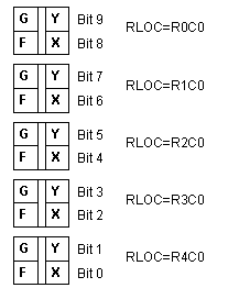
|
Following Xilinx's standard, the two main
function generators are shown on the left of diagrams, and are labeled F
and G, and the two flip-flops are shown on the right and are labeled X and
Y.
For the example counter, in the CLB at the bottom of the
five CLB group (the one with the RLOC=R4C0 attribute), the F function
generator will be used to implement the logic that feeds the D pin of the
X flip-flop, the output of which, is the least significant bit of the
counter, Q0.
The G and Y sections of the same CLB implement bit 1 of
the counter. The next CLB above (the one with the RLOC=R3C0 attribute)
implements bit 2 and 3. This continues up the column, through to the top
CLB which implements bits 8 and 9. | When two or more functions of your design are Floorplanned in
this way and placed side by side, with the signals that flow from one function
to the next aligned on the same row, and in near or adjacent columns, the design
will place and route much faster and the resulting design will perform faster
than a design without Floorplanning, and that relies on the Xilinx place and
route software to decide on placement. Of course, custom building each function
section of your design with detailed Floorplanning for each function generator
and flip-flop can be a complex, time consuming, and potentially error prone
process.
The Xilinx Place and Route software uses a hierarchical placement
constraint system called relative location attributes. Each level of the
hierarchy has an origin in the top left corner that has a relative location of
row zero and column zero. As a constraint this is represented as R0C0. Rows are
numbered from top to bottom, and columns are numbered from left to right. When a
relative location attribute (RLOC) is assigned to a part of the hierarchy that
is not a single CLB, then the underlying RLOCs are added to the attached
attribute to calculate the RLOC value for each of the underlying RLOCs. This
process continues throughout the hierarchy, resolving each CLB RLOC to a value
that is relative to the RLOC at the top of the hierarchy. This process, and
other issues related to how RLOCs are processed are discussed in full in the
Xilinx "Libraries Guide" document, in the "Attributes, Constraints, and Carry
Logic" chapter, in the "Relative Location (RLOC) Constraints" section. Although
this section of Xilinx's documentation is quite complex, it is recommended that
you review it to better understand how the RLOCs in the modules support
Floorplanning.
An Example design, with various levels of Floorplanning
This section examines the results of Floorplanning, and compares
the resulting structure, the place and route time, and the design performance.
The example while contrived is typical of the types of logic that benefit from
Floorplanning. The example design comprises four sixteen bit binary up counters,
that all feed into a selection multiplexer. The output of the selection
multiplexer is registered, and the output of this register is connected to the
FPGA pins.
There are two basic timing path categories that need to be
analyzed. The first is the maximum delay in any of the counters. And the second
is the maximum delay from any of the counters to the multiplexer output
register. For the counter, the maximum delay will be from the clock to out time
of the LSB flip-flop, through the logic that establishes the next counter value,
to the D input of the MSB flip-flop, and meeting its setup time. The reciprocal
of this maximum internal delay within the counter is the maximum clock rate at
which the counter will count reliably.
Seven different levels of Floorplanning are applied to this
simple design, using the XC4005E, XC4010E, and XC4010XL as targets. The '-2'
speed grade is used for all examples, and place and route programs used are as
follows:
- XC4005E-2 PPR V5.2.1
- XC4010E-2 PPR V5.2.1
- XC4010E-2 PAR M1.4
- XC4010XL-2 PAR M1.4
The combination of running the XC4010E devices with both place
and route programs allows comparison of these programs on the XC4000E families.
Running both the XC4010E and XC4010XL on the M1.4 program, allows comparison of
these two product families. While the goal is to show the value of
Floorplanning, the program and product comparisons are
interesting.
The same seven levels of Floorplanning were applied to each of
these four product/program combinations. The seven design styles have the
following characteristics:
- The
4 counters are binary ripple counters (CB16CE), from the Xilinx unified
library XC4000E, the multiplexer and output register are also taken from this
library. There is no Floorplanning in this style, and the choice of a ripple
counter, while available in the library, is a poor
choice.
- The
4 counters are binary counters that use the built-in carry logic (CC16CE),
from the Xilinx unified library XC4000E, the multiplexer and output register
are also taken from this library. While there is no explicit Floorplanning in
this style, the counters include internal Floorplanning, because the carry
logic imposes a column structure on the counters.
- This
style adds four RLOC_ORIGIN Floorplanning constraints to the style 2 design,
placing the four counters in adjacent column, and aligning the MSBs of the
counters (and all other bits).
- This
style replace the un-Floorplanned output register of the previous styles with
a Floorplanned register, and places it in the column to the right of the
fourth counter. It also is aligned with regard to bit
positions.
- This
style is like style 4, except the output register is placed in the column to
the right of the column used for the register in style 4.
- This
style uses a Floorplanned multiplexer and output register, and places it in
the two columns to the right of the fourth counter. The odd bit multiplexers
and output register flip-flops are in one of these two columns, and the even
bits are in the other column.
- This
style uses the same components of style 6, but the Floorplan has been changed.
The first two columns contain the first two counters, the next two columns are
the multiplexer and output register, and the last two columns contain the
third and fourth counter.
To understand the differences in the results for these design
styles, the following descriptions of the behavior of the place and route
software, as well as an analysis of the device resources should be
helpful.
Style 1 uses no Floorplanning or guidance on using the carry
logic that is available in these products. The results are consistently the
poorest. Style 2 changes the structure of the counters to use carry logic, and
for this style through to style 7, the performance and size of the counters does
not change much. There is no direct Floorplanning of the counters with regard to
their relative placement. While this does not affect the counters, it may not be
optimal for the routing from the counters to the multiplexer. As can be seen in
the following diagrams, the style 2 designs have placed the counters near each
other, but they are not aligned.
Style 3 adds Floorplanning to the counters, and by aligning the
counters, the routing to the multiplexer should be more straightforward. This
should improve the delays from the counters through the multiplexer to the
output register. As can be seen in the diagrams, the multiplexer logic is placed
somewhat randomly around the core of the 4 counters.
Style 4 places the output register in the next column to the
right of the four counters, and the flip-flops of this register are aligned with
the counter bits. Although this should help significantly, it does not, because
the 8 logic blocks that hold the 16 flip-flops of the output register do not
have sufficient gate resources to implement the 16 four-input multiplexers. Some
of the multiplexers are placed with the flip-flops, and some are placed near
by.
Style 5 attempts to alleviate the problems with style 4, by
moving the output register to the next column to the right, leaving room for the
8 multiplexers that couldn't fit in with the flip-flops. None of the place and
route programs take full advantage of this opportunity for
improvement.
Style 6 resolves the performance issue of the multiplexer, by
replacing it with a Floorplanned multiplexer with output register. This
multiplexer performs an additional optimization of not placing all the
flip-flops in the same column, but rather, placing the flip-flops with the
multiplexers. A four-to-one multiplexer requires all the gate resources of a
CLB, so to build a 16 bit wide multiplexer with four inputs will require 16
CLBs. Strictly maintain a Floorplanning structure of two bits of data path
implemented per row of structure. The 16 CLBs are Floorplanned to use two
columns by eight rows, with bits 0 and 1 on the row at the bottom, and bits 14
and 15 at the top. This exactly matches the bit position of the counters, except
the counters have an additional block at the top, for the TC and CEO outputs.
This is resolved by placing the counters with RLOC-ORIGINS on row 1, but the
multiplexer is placed on row 2.
At this point you may wonder what additional improvement could be
made to style 6. Consider the routing from the left most counter to the
multiplexer. It must pass through the other three counters to get to the
multiplexer. Similarly, the output of counters two and three must also pass
through the fourth counter to get to the multiplexer. Therefore, there is more
routing congestion around counter four, although it has the shortest path to the
multiplexer. The output of the first counter must traverse the furthest distance
to get to the multiplexer. In synchronous designs like this, the slowest path
out of a group of paths will be the limiting factor. For the counters to run at
their fastest, they need to have their routing congestion minimized. For the
paths from the four counters to the multiplexer to be minimized, the multiplexer
and the four counters need to be placed so as to minimize the worst-case
distance. Both of these goals are achieved in style 7 by placing the multiplexer
and its output register in the middle of the structure, with two counters to its
left, and two counters to its right.
As can be seen from the following tables and diagrams, style 7
delivers the fastest counters, the fastest counter to multiplexer output
register time, the fastest placement time, and the fastest routing time.
Studying the schematics for design styles 1 and style 7 shows almost no
additional effort to create design 7's result. Selecting counters and
multiplexers that are pre-Floorplanned, together with five placement attributes
is all that is required. (Some thought as to what the placement constraints
should be, obviously is also needed)
|
XC4005EPC84-2 Processed with PPR
V5.2.1c |
|
Design Style |
Counter Delay (nS) |
Max Frequency (MHz) |
Counter to MUX REG delay
(nS) |
Partition + Placement time
(S) |
Routing Time (Seconds) |
CLBs Used |
|
1 |
17.1 |
58.4 |
11.8 |
4+28 |
12 |
72 |
|
2 |
13.1 |
76.3 |
10.8 |
6+15 |
13 |
48 |
|
3 |
13.4 |
74.6 |
11.7 |
6+14 |
17 |
48 |
|
4 |
13.1 |
76.3 |
14.4 |
7+12 |
17 |
48 |
|
5 |
14.3 |
69.9 |
14.5 |
6+12 |
16 |
48 |
|
6 |
13.3 |
75.1 |
9.4 |
3+11 |
16 |
48 |
|
7 |
13.1 |
76.3 |
8.9 |
3+11 |
14 |
48 |
|
XC4010EPC84-2 Processed with PPR
V5.2.1c |
|
Design Style |
Counter Delay (nS) |
Max Frequency (MHz) |
Counter to MUX REG delay
(nS) |
Partition + Placement time
(S) |
Routing Time (Seconds) |
CLBs Used |
|
1 |
17.5 |
57.1 |
12.9 |
7+53 |
32 |
88 |
|
2 |
13.3 |
75.1 |
11.2 |
4+13 |
12 |
48 |
|
3 |
13.5 |
74.0 |
12.6 |
4+11 |
15 |
48 |
|
4 |
13.1 |
76.3 |
14.6 |
4+11 |
17 |
48 |
|
5 |
13.2 |
75.7 |
14.2 |
3+11 |
14 |
48 |
|
6 |
13.3 |
75.1 |
10.2 |
2+10 |
16 |
48 |
|
7 |
13.1 |
76.3 |
8.9 |
1+10 |
15 |
48 |
|
XC4010EPC84-2 Processed with
M1.3.7 (PAR –L4 –D5) (A) |
|
Design Style |
Counter Delay (nS) |
Max Frequency (MHz) |
Counter to MUX REG delay
(nS) |
Placement time
(Seconds) |
Routing Time (Seconds) |
CLBs Used |
|
1 |
21.9 |
45.6 |
19.4 |
65-7=58 |
574-65=509 |
55 |
|
2 |
13.7 |
72.9 |
10.0 |
47-7=40 |
142-47=95 |
48 |
|
3 |
13.8 |
72.4 |
10.3 |
38-8=30 |
170-38=132 |
48 |
|
4 |
13.8 |
72.4 |
12.7 |
28-8=20 |
132-28=104 |
56 |
|
5 |
13.7 |
72.9 |
13.1 |
28-8=20 |
128-28=100 |
56 |
|
6 |
13.7 |
72.9 |
9.4 |
15-8=7 |
80-15=65 |
48 |
|
7 |
13.7 |
72.9 |
8.9 |
14-8=6 |
75-14=61 |
48 |
|
XC4010XLPC84-2 Processed with
M1.3.7 (PAR –L4 –D5) (B) |
|
Design Style |
Counter Delay (nS) |
Max Frequency (MHz) |
Counter to MUX REG delay
(nS) |
Placement time
(Seconds) |
Routing Time (Seconds) |
CLBs Used |
|
1 |
18.5 |
54.0 |
8.8 |
68-20=48 |
147-68=79 |
55 |
|
2 |
11.6 |
86.2 |
7.0 |
53-21=32 |
134-53=81 |
48 |
|
3 |
11.9 |
84.0 |
6.9 |
46-21=25 |
128-46=82 |
48 |
|
4 |
12.1 |
82.6 |
10.6 |
34-22=12 |
95-34=61 |
56 |
|
5 |
11.7 |
85.4 |
10.7 |
33-21=12 |
91-33=58 |
56 |
|
6 |
11.9 |
84.0 |
6.8 |
25-20=5 |
64-25=39 |
48 |
|
7 |
11.7 |
85.4 |
6.1 |
26-21=5 |
69-26=43 |
48 |
|
XC4010XLPC84-2 Processed with
M1.4.12 (MAP –K, PAR –L4 –D5) |
|
Design Style |
Counter Delay (nS) |
Max Frequency (MHz) |
Counter to MUX REG delay
(nS) |
Placement time
(Seconds) |
Routing Time (Seconds) |
CLBs Used |
|
1 |
18.2 |
54.9 |
11.3 |
64-20=44 |
185-64=121 |
83 |
|
2 |
11.3 |
88.5 |
9.8 |
39-21=18 |
183-39=144 |
72 |
|
3 |
11.8 |
84.7 |
10.6 |
33-20=13 |
108-33=75 |
72 |
|
4 |
11.6 |
86.2 |
10.8 |
32-21=11 |
128-32=96 |
72 |
|
5 |
11.7 |
85.4 |
11.0 |
32-21=11 |
116-32=84 |
72 |
|
6 |
11.6 |
86.2 |
6.8 |
24-21=3 |
59-24=35 |
48 |
|
7 |
11.7 |
85.4 |
6.1 |
24-20=4 |
61-24=37 |
48 |
|
XC4010XLPC84-2 Processed with
M1.4.12 (MAP –K, PAR –L5 –D5) |
|
Design Style |
Counter Delay (nS) |
Max Frequency (MHz) |
Counter to MUX REG delay
(nS) |
Placement time
(Seconds) |
Routing Time (Seconds) |
CLBs Used |
|
1 |
17.3 |
57.8 |
11.3 |
99-20=79 |
224-99=125 |
83 |
|
2 |
11.7 |
85.4 |
9.9 |
58-21=37 |
229-58=171 |
72 |
|
3 |
12.1 |
82.6 |
10.5 |
46-20=26 |
140-46=94 |
72 |
|
4 |
11.6 |
86.2 |
11.1 |
44-21=23 |
117-44=73 |
72 |
|
5 |
11.7 |
85.4 |
10.9 |
44-21=23 |
134-44=90 |
72 |
|
6 |
12.1 |
82.6 |
6.7 |
27-21=6 |
60-27=33 |
48 |
|
7 |
11.7 |
85.4 |
6.1 |
27-21=6 |
66-27=39 |
48 |
|
XC4010XLPC84-2 Processed with
M1.4.12 (PAR –L4 –D5) |
|
Design Style |
Counter Delay (nS) |
Max Frequency (MHz) |
Counter to MUX REG delay
(nS) |
Placement time
(Seconds) |
Routing Time (Seconds) |
CLBs Used |
|
1 |
18.8 |
53.2 |
9.1 |
63-20=43 |
199-63=136 |
55 |
|
2 |
12.0 |
83.3 |
7.7 |
45-20=25 |
132-45=87 |
48 |
|
3 |
12.2 |
81.9 |
6.7 |
36-21=15 |
116-36=80 |
48 |
|
4 |
11.9 |
84.0 |
10.3 |
30-20=10 |
97-30=67 |
56 |
|
5 |
12.0 |
83.3 |
10.5 |
31-21=10 |
103-31=72 |
56 |
|
6 |
11.6 |
86.2 |
6.8 |
24-20=4 |
58-24=34 |
48 |
|
7 |
11.7 |
85.4 |
6.1 |
24-20=4 |
61-24=37 |
48 |
|
XC4010XLPC84-2 Processed with
M1.4.12 (PAR –L5 –D5) |
|
Design Style |
Counter Delay (nS) |
Max Frequency (MHz) |
Counter to MUX REG delay
(nS) |
Placement time
(Seconds) |
Routing Time (Seconds) |
CLBs Used |
|
1 |
18.1 |
55.2 |
7.7 |
105-21=84 |
257-105=152 |
55 |
|
2 |
12.0 |
83.3 |
6.7 |
72-21=51 |
199-72=127 |
48 |
|
3 |
11.8 |
84.7 |
6.8 |
55-21=34 |
138-55=83 |
48 |
|
4 |
12.1 |
82.6 |
10.5 |
40-21=19 |
148-40=108 |
56 |
|
5 |
12.1 |
82.6 |
10.6 |
40-20=20 |
102-40=62 |
56 |
|
6 |
12.1 |
82.6 |
6.7 |
29-22=7 |
61-29=32 |
48 |
|
7 |
11.7 |
85.4 |
6.1 |
27-21=6 |
66-27=39 |
48 |
Interpreting the Floorplan Pictures
The full
manual has all the pictures for all 8 of the above tables of data. This page
only has the pictures for the last table, Which is the M1 PAR V1.4.12, with -L 5
and -D 5, which represent high effort in both placer and router.
At the
time of writing this page, the XC4000XL is Xilinx's leading FPGA family, and the
M1 PAR version 1.4.12 is the current version of the place and route software.
The color
coding of the following Floorplans is as follows:
All the pictures are of
XC4010XL devices, which is an array of 20 by 20 CLBs. These are represented by
small squares. If it is empty, the CLB is not usedWithin each CLB, colored
squares on the left are F & G function generators, colored squares on the
right are the flip-flops, and a colored rectangle in the middle represents the H
function generator.If a square is colored
blue, then it is being usedIf a square is colored
yellow, then it is a function generator, and the carry logic is
activeIf a square is colored
magenta, then it is a function generator, and it is being used for single ported
RAMIf a square is colored red,
then it is a function generator, and it is being used for dual ported
RAMIf a square is colored
green, then it is a function generator, and it is being used for
ROMIf an I/O cell is colored
red, then it is being used for a global clock bufferAn "X" over an I/O cell
indicates an I/O cell that is not bonded to a package pinAn inward pointing arrow on
an I/O cell indicates usage as an inputAn outward pointing arrow
on an I/O cell indicates usage as an outputIf an I/O or CLB cell has a
gray background, then it means that there was placement control used on that
location
|
|
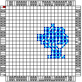
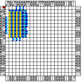
XC4010XL-S1-F
The 4 counters are binary ripple counters (CB16CE), from the Xilinx
unified library XC4000E, the multiplexer and output register are also
taken from this library. There is no Floorplanning in this style, and the
choice of a ripple counter, while available in the library, is a poor
choice.
This is also what you will get from synthesis if it does
not know about the carry logic in the XC4000 families.
|
|
|
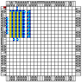
XC4010XL-S2-F
The 4 counters are binary counters that use the built-in carry logic
(CC16CE), from the Xilinx unified library XC4000E, the multiplexer and
output register are also taken from this library. While there is no
explicit Floorplanning in this style, the counters include internal
Floorplanning, because the carry logic imposes a column structure on the
counters.
This is also what you will get from synthesis if it
knows about carry logic, but you do not do any Floorplanning. While the
performance for this style is not too bad for this example, when a chip is
used at 50% or more, the lack of Floorplanning can seriously degrade
performance, and routing times may become very long.
|
|
|
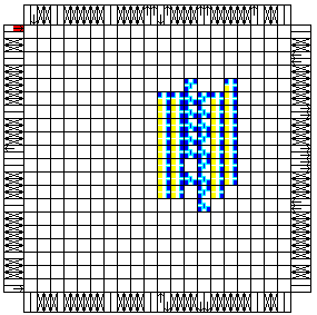
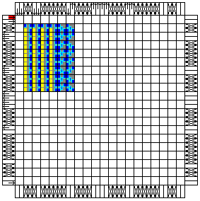
XC4010XL-S3-F
This style adds four RLOC_ORIGIN Floorplanning constraints to the style
2 design, placing the four counters in adjacent column, and aligning the
MSBs of the counters (and all other bits).
The Floorplanning is
shown by the gray background to the four columns that contain the
counters. Since the multiplexer is not Floorplanned, it is the CLBs with
logic in them, but a white
background.
|
|
|
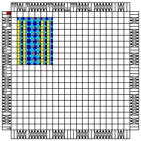
XC4010XL-S4-F
This style replace the un-Floorplanned output register of the previous
styles with a Floorplanned register, and places it in the column to the
right of the fourth counter. It also is aligned with regard to bit
positions.
Note that the multiplexer logic is still scattered all
around the Floorplanned core. Although there is room in the Floorplanned
output register CLBs to merge some of the multiplexer, the mapper in the
current version of the M1 software will not do this.
|
|
|
XC4010XL-S5-F
This style is like style 4, except the output register is placed in the
column to the right of the column used for the register in style 4.
This opened up a column for the placer to move the multiplexer
into. It looks like half of the 16 bits of multiplexer logic have been
moved into this area, and half are still floating about. Merging the
multiplexer into the Floorplanned output register CLBs has not happened.
|
|
|
XC4010XL-S6-F
This style uses a Floorplanned multiplexer and output register built by
FlibGen module
generator, and places it in the two columns to the right of the fourth
counter. The odd bit multiplexers and output register flip-flops are in
one of these two columns, and the even bits are in the other column. |
|
|
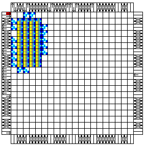
XC4010XL-S7-F
This style uses the same components of style 6, but the Floorplan has
been changed. The first two columns contain the first two counters, the
next two columns are the multiplexer and output register, and the last two
columns contain the third and fourth
counter. |
If you have read this page
and found it useful, please send an email to philip@fliptronics.com
Copyright ?1998,
1999, 2000, 2001, 2002 by Fliptronics. All rights
reserved.
Fliptronics, Sunnyvale, CA 94086-7629, USA
TEL: 408-737-0295, E-mail:
philip@fliptronics.com
|