![]()
작성일: 2001.07.23
[Prof.Ben-Avi]
(We shall now take a quick initial tour through the land of PLDs.... the devices selected for this introductory tour have been chosen either because they are/were extremely popular or because they have/had particularly useful features that are/were also found in other devices. First let's discuss the different architectures of these devices. The architecture of a PLD affects the logic applications for which the device can be used. Currently, there are about 300 unique architectures of PLDs available. This number is constantly growing as manufacturers introduce new devices... I'll conclude this handout with an overview of current PLD technologies. Technology attributes include such things as manufacturing process (CMOS, bipolar, ECL, and so on), package type, speed grade, eraseability, and so forth. If we factor in all the available technology options, the number of distinct PLD's available rises into the many thousands. Technology differences affect how a programmed device will operate in a larger circuit, how the device is actually programmed, and in what kind of systems it can be utilized.)
When we refer to the architecture of a PLD, we are referring to those device attributes that affect the logical construction of the device -- those attributes significant to the logic of a design to be implemented. Architectural attributes include such things as the configuration of the pins, the arrangement and size of the programmable array(s), and the configuration of the input and output interface logic.
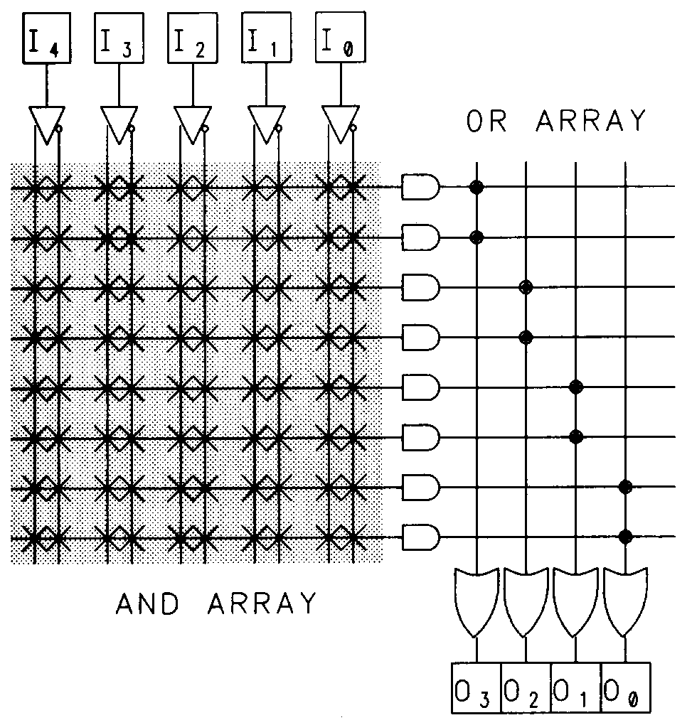
A programmable logic array is normally composed of a specific number of input lines connected through a fixed or programmable array to a set of AND gates, which are in turn connected to a fixed or programmable array of OR gates. The OR gates provide the output signals from the logic array.
A simplified programmable logic array composed of two inputs and one output is shown in Figure 1.
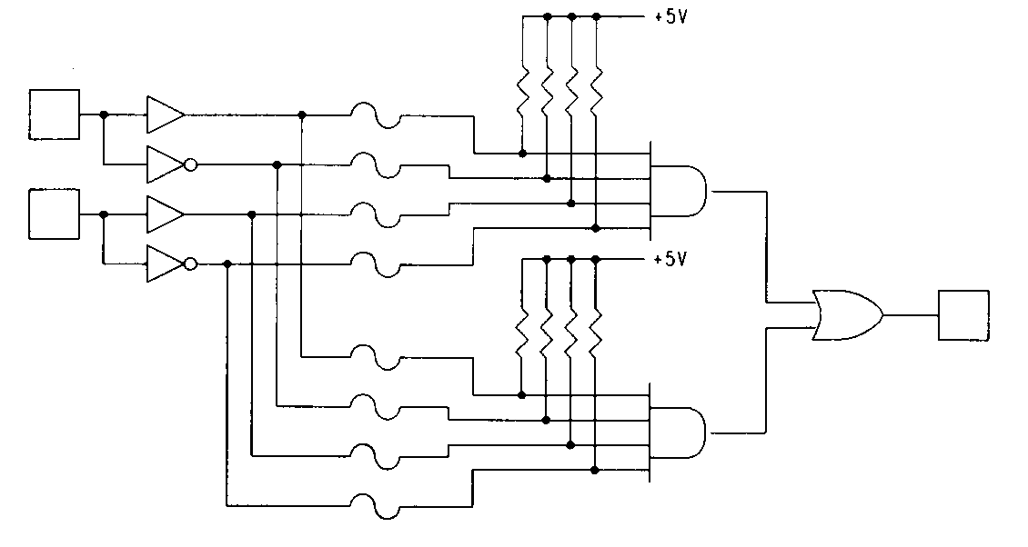
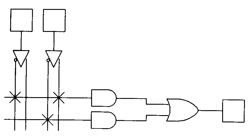
Notice that, to provide all possible combinations of inputs, each input is routed to the array in both its true and complemented form. These inputs are then connected to AND gates via programmable interconnection points. These product terms are OR-ed together to form a sum-of-products logic array. Since a typical PLD has many more inputs and outputs than the simple array shown above, a special notation, called a logic diagram, is used to graphically describe the complex PLA structures associated with these devices. When the array is programmed to implement a particular logic function, the desired inter-connections can be indicated on the logic diagram with Xs. Figure 2 shows the two-input, one output logic array drawn in logic diagram form and programmed with a simple logic function.
In some devices, the AND/OR structure is replaced by either NAND/NAND or NOR/NOR structures, (... remember de'Morgan's laws?? Remember EE150?? Remember your name??), but the result is the same: with a large enough array, any logic function can be implemented.
Programming of the device is accomplished by enabling or disabling interconnections in the device's programmable array. The actual connections can be provided in a variety of ways depending on the device technology.
Programmable read-only memories (PROMs) are the oldest form of programmable logic devices, but were not actually designed for logic applications. PROMs have historically been used to store data such as boot-strap programs and micro-code instructions. They have also been used extensively for decoding functions and simple state machines (when provided with external storage registers) and as such can be considered programmable logic devices. The PROM structure can be used for any general purpose logic circuit since it incorporates a sum-of-products logic array. The basic PROM array is shown in the logic diagram of Figure 3.
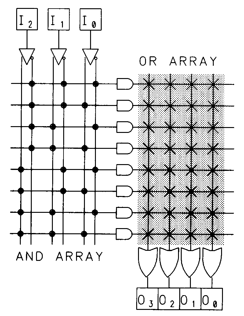
In this figure, all programmable fuse locations are indicated with Xs. To program this PROM array, you decide which of the interconnect points (each intersection of a horizontal and vertical line) are to be preserved, and disable the remaining connections. For a PROM with n inputs, there are 2n possible input values, all of which are provided for in the AND array. The programmable OR array allows each of these input values to be decoded into any value consisting of k outputs, where k equals the number of OR gates (and corresponding outputs) in the array. This makes PROMs particularly well suited for read-only memory applications and this is their most common use. Since a PROM can map any of its input states into an arbitrary output state, it can be used quite effectively for implementing n-input, k-output combinational logic functions. Each unique input state corresponds to one unique product term in the array.
To use a PROM for logic functions, the designer need only specify the truth table for the set of functions. There is no need for logic minimization since all possible input combinations are provided in the AND array. As we pointed out, a PROM provides the complete set of input combinations in the AND array. For most logic functions, however, this is completely unnecessary, and results in a tremendous amount of wasted circuitry on the chip. Particularly, when a large number of inputs are required, the PROM structure becomes impractical. Consider, for example, when a logic function of sixteen input variables and eight output variables is desired. To implement such a function in a PROM, you would have to use a 64K by 8 bit PROM device, regardless of the complexity of the logic function. A PROM of this size would be a highly inefficient vehicle for most logic functions. Most n-variable logic functions can be implemented with far less than 2n product terms. To more efficiently map logic functions with a larger number of inputs, the PLA (programmable logic array) and PAL (programmable array logic) devices were developed. The PLA structure is the basis for virtually all PLDs in use today. The complete PLA structure is the basis for a variety of PLDs, and provides the greatest flexibility in how product terms are allocated to the OR gates and associated outputs. The PLA structure, shown in figure 4, features both a programmable AND-array, and a programmable OR array.
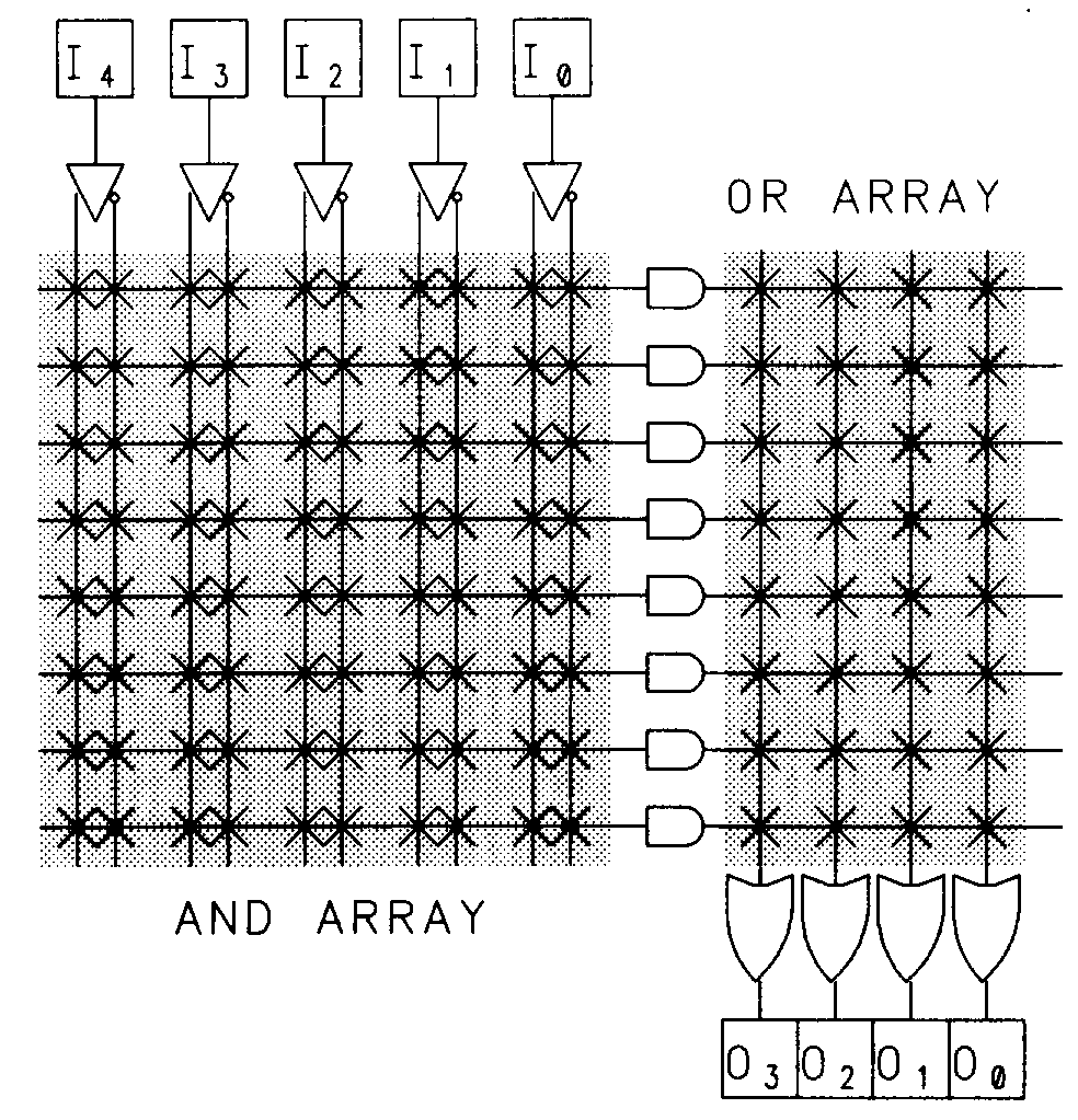
For a PLA with n inputs, any input variable (or its complement) may be an input to any AND gate. Therefore, any AND gate in the AND array can be configured to implement any of 3n possible product terms (3n because each input to an AND gate has three possible values true, complement, and no-connect). The design of the PLA allows any product term in the array to be connected to the OR gate of any output. This feature is sometimes referred to as product-term-sharing. The PLA provides the most flexibility for implementing logic circuits, particularly for large designs in which many common logic elements can be shared between circuit outputs.
PLA type devices are generally slower in operation than PROMs and PALs since there are two programmable arrays through which signals must propagate. Unlike a PROM, the total number of product terms available in a PLA is limited, so logic minimization is important when implementing designs. The PAL (programmable array logic) structure is similar to the PLA, but has a fixed OR array, as illustrated in Figure 5.
Every output in a standard PAL-type device has one OR gate that is unique to that output. There is no provision for product term sharing (although, as we shall see later, some PAL-based devices do allow for various forms of product term reallocation). These product terms are then gated together by fixed OR gates to drive the device outputs. As I said, since a limited number of product terms are provided for each PAL output, logic minimization techniques become important when logic circuits are implemented in PAL devices.
The most common PALs in use today are the 16L8 and 16R4/6/8 series of devices. These 20-pin devices originated at MMI (now a part of AMD) are now available from many manufacturers. The devices are intended to replace standard logic parts and are, therefore, designed to operate with TTL (transistor-transistor logic) signal levels -- you can interconnect them freely with 74LSxx series chips from your EE150 kit.
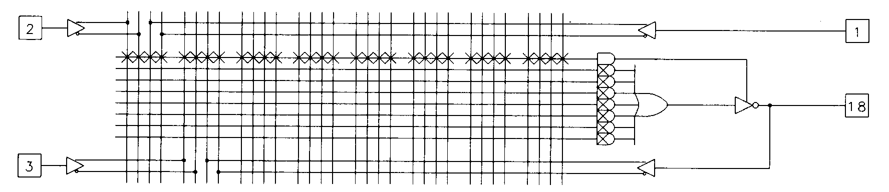
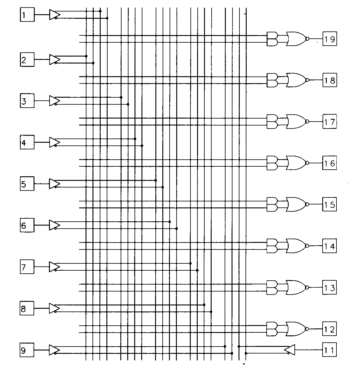
Combinational PALs are those devices that are based on a PAL structure, and do not contain any memory elements. Combinational PALs are useful for a wide variety of random logic functions, including decoders, interface logic, and other applications that require a simple decoding of device inputs. The 16L8 represents the typical combinational PAL and is diagrammed in Figure 6.
The diagram for the 16L8 shows that the device has ten dedicated inputs (pins 1 through 9 and pin 11) to the programmable AND array. Each input to the array is available in its true or complemented form allowing any combination of the inputs to be expressed on any row of the array. Each row of the 16L8 array corresponds to one product term of the device. The 16L8 has eight outputs, each of which is fed by a seven-input OR gate. Each output of this device is capable of implementing a logic function composed of seven or fewer product terms. The eighth product term is used to control the three-state output buffer, the function of which we will examine in a moment.
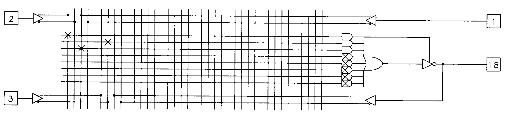
A simple logic function is shown implemented in the 16L8 in Figure 7(a).
The X's shown on the diagram indicate fuse interconnections that have been left intact to implement the function. A large X inside of an unused AND gate indicates that all of the fuses for that row are to be disconnected. When all of the fusible links for a row are disconnected, the associated OR gate input floats high. Figure 7(b) shows the same logic function expressed as a traditional schematic.
Notice that there is an inverter associated with the PAL output. There are PAL devices available that don't have the output inverter (often indicated with an H in the part name, such as, 16H8 instead of 16L8) but these devices are less frequently used since active-low logic is prevalent and these logic functions normally fit better in a PLD with inverted outputs. In addition to the dedicated inputs, there are six I/O pins (pins 13 through 18) on the device that may be used as array inputs as well. These pins can be used in a variety of ways. To use these I/O pins as dedicated inputs, you must disable the three-state output buffer associated with that pin. When a three-state buffer appears on the output of a PLD, it's called an output enable.
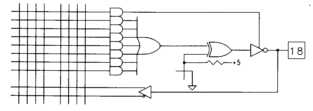
Since the output enable for the 16L8 is controlled from the array, you disable it by leaving intact the fuses for the dedicated product term that controls the enable. Leaving all of the fuses intact (or, for that matter, any pair of true and complement array inputs for a single input pin) for any product term in the device results in a logic level 0 on that product term. This is shown in Figure 8.
Using the I/O pins as inputs, it's possible to use the 16L8 to implement logic functions with as many as sixteen separate inputs, at the expense of usable outputs. The I/O pins can also be used as dedicated outputs, by permanently enabling the output enable. This is done by blowing all of the fuses for the output enable's product term as was done in Figure 7(a). When all of the inputs to an AND gate in this device are disconnected, the AND gate floats high, in this case, enabling the output enable. When the output enable of a 16L8 I/O pin is enabled, the input to the array is still active, and can be used to feed the output back into the array. This is useful for multilevel logic applications (see later handouts). This feature can also be used to create oscillating or asynchronous sequencer circuits, although these applications aren't generally recommended. The most common use of the output enable is for traditional three-state purposes such as bus interfacing. To use the output enable dynamically, you simply program the output enable product term with the desired logic as shown in Figure 9.
Quite often, there are situations in which a design be implemented in a 16L8 or 16H8 due to the need for some of the outputs to be inverted while others are not. For these applications, a version of the 16L8 is available, called the 16P8 that has a feature called programmable output polarity. Figure 10 illustrates how programmable output polarity is implemented in the 16P8 device. To provide programmable output polarity, each output of the 16P8 includes an XOR gate. One input to this XOR is the output of one of the PAL's OR gates, while the other can be either connected to ground through a fuse or disconnected and allowed to float high. Some devices utilize other methods such as multiplexers or transmission gates for polarity control, but the result is the same.
There are a wide variety of simple PALs that have architectures similar to the 16L8. Most of these are stripped down versions that are somewhat less expensive. One of the least complex of these PALs is the 10L8, illustrated in Figure 11.
This device has only dedicated input and output pins, no output enable, and no feedback lines. The small number of product terms (sixteen total) and small number of inputs means that this device has only 320 fuses, and is only slightly more complex than a simple 32 by 8-bit PROM device. These smaller PAL devices are rapidly losing popularity, as most PLD users find that it's most economical (because of inventory costs) to use the 16L8 or 16P8 for all of their strictly combinational applications, rather than attempt to save a few pennies per device by using simpler PAL devices.
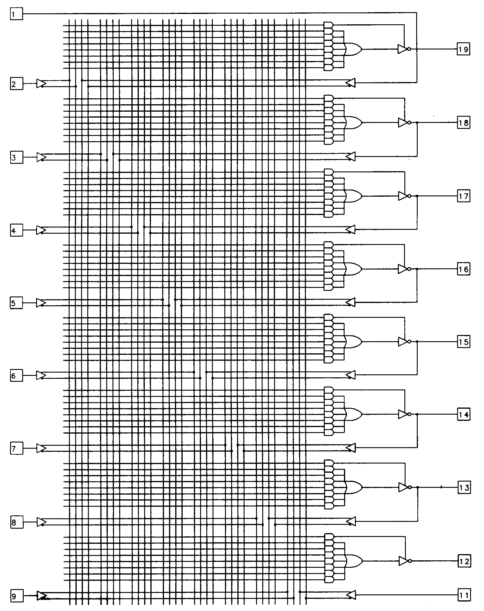
The most commonly used registered PAL devices are represented by the 16R4, the 16R6, and the 16R8 devices. The 16R4 device is shown in Figure 12.
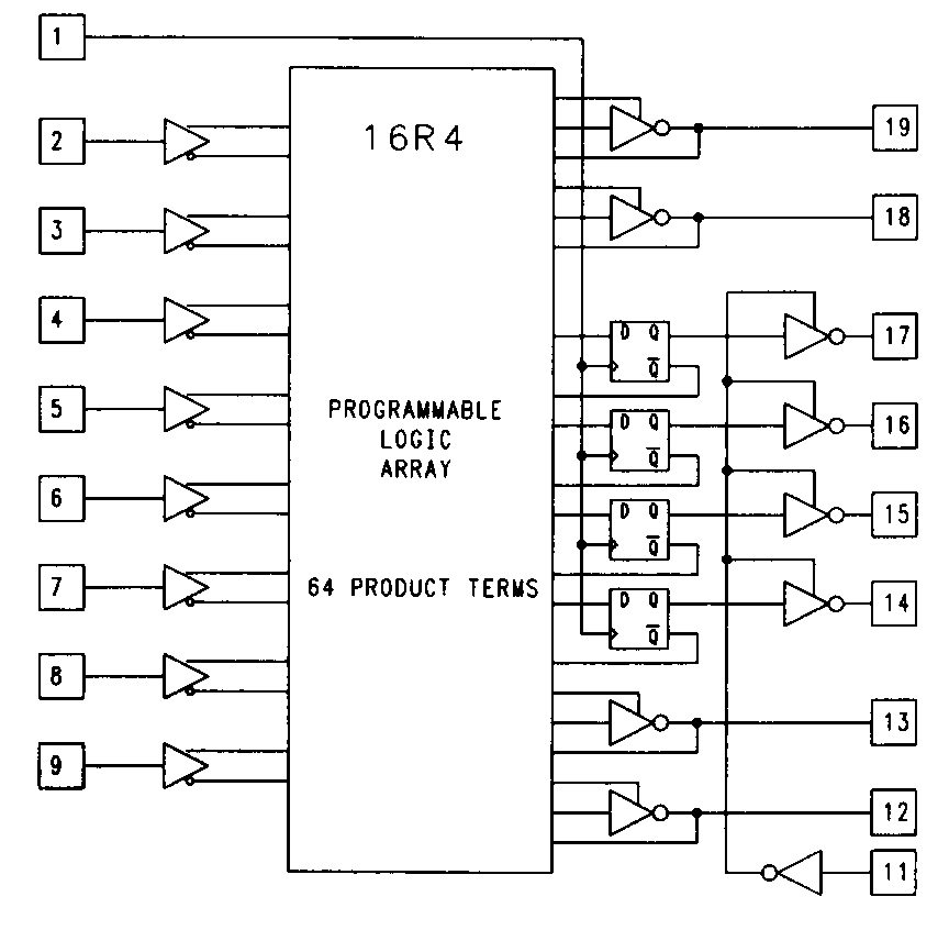
The design of the 16R4 device is similar, in most respects, to that of the 16L8. The difference is found on output pins 14 through 17. These outputs feature edge-triggered D-type flip-flops. The Q output of each flip- flop is routed to the PAL output through the output enable and each flip-flop's ¬Q output is routed back to the AND array. Like the fed-back combinational signals on the other outputs, these signals are provided to the array in both their true and complement form.
The flip-flops are all controlled by a common clock which is tied directly to pin 1 on the device. This implies, of course, that pin 1 be used as an input, as it can in the 16L8. This is also true of pin 11, which is used as a dedicated input for the output enable of the flip-flops.
This method of enabling outputs is common to most of the simpler PAL devices. In general, combinational outputs are enabled from a product term, while registered outputs are enabled from a dedicated pin. Since no product term is used for the output enable of the registered outputs, the eighth product term is made available for use as an input to the OR gate for those outputs. For most applications that require output synchronization or state memory, the output enable feature will be used globally, so a complex output enable is not required. Another trade-off in the design of these devices' output enables is speed; a pin controlled output enable will have a faster pin-to-enable speed. The architecture of the 16R4 is well suited for simple state machine applications. The registered outputs can be dedicated for use as state memory registers, while the combinational outputs can be used for either state machine outputs or additional control inputs. Note that it isn't possible to use the registered output pins of the 16R4 as inputs under any circumstances.
To show how devices like the 16R4 are used for sequential designs, we will implement a simple circuit. This design is a simple 4-bit counter, the Boolean equations for which are shown in Figure 13.
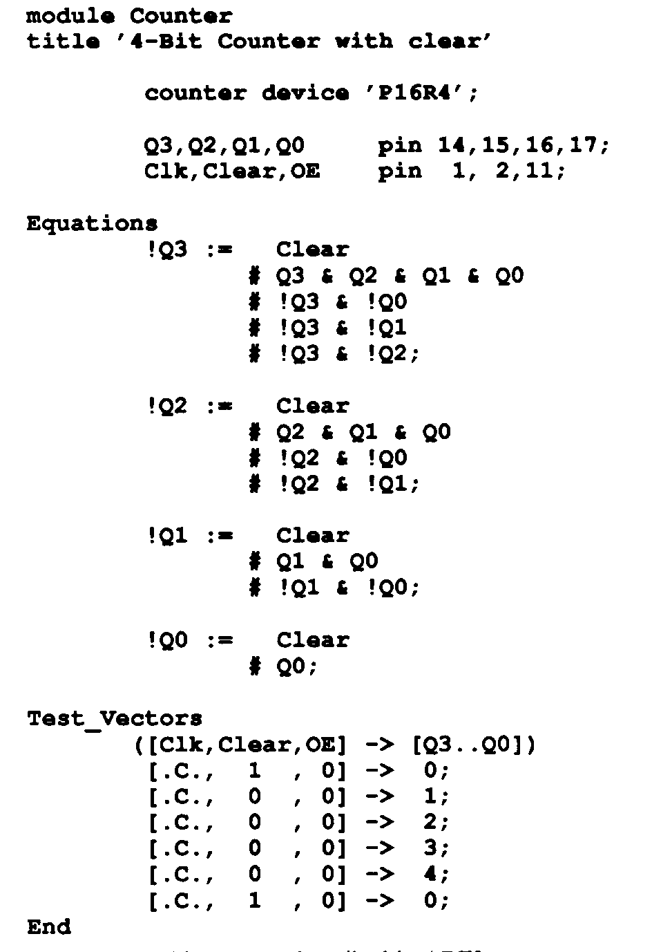
The design file shown is written in the ABEL -- similar to OrCAD -- language and uses simple Boolean equations that represent the logic of the counter. In ABEL, the & symbol represents an AND operation, the # symbol represents an OR operation, and the ! symbol represents a NOT operation.
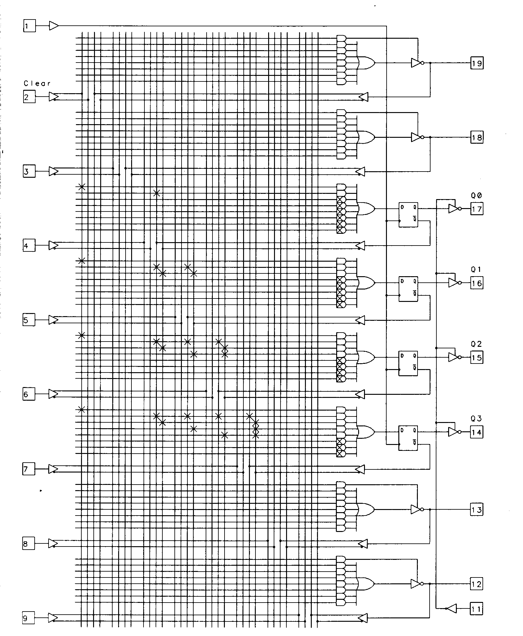
How these equations were derived is not important -- you know how to design a synchronous counter from EE150; we won't go into the specifics of this counter design here. Simply accept the fact that this counter increments a 4-bit number by one every time the device is clocked. The design utilizes active low logic, so the values observed on the device's outputs will be the complement of the actual number stored in the registers. Figure 14 is the device.
The least significant bit of the counter (represented by the Q0 variable in the counter equations) is mapped to pin 14 of the device and requires the least logic of any of the counter outputs -- this is typical. The remaining bits of the counter, Q1 through Q3, require correspondingly more logic, since they must each decode the previous counter bits to determine whether a change in state is required.
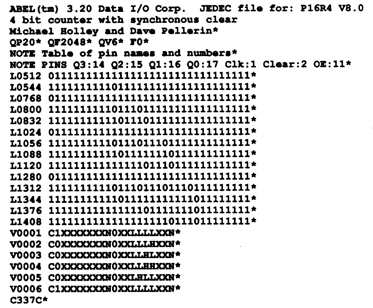
The JEDEC standard format file that corresponds to the counter design is shown in Figure 15. This file is created by ABEL (or OrCAD) and is used to download programming data to a device programmer. The rows of ones and zeroes represent fuse locations and corresponding fuse values where a one indicates a blown fuse and a zero indicates an intact fuse.
A timing diagram of the counter circuit is shown in Figure 16. The diagram shows the relationship between the 16R4's clock input and the resulting counter-values appearing on the counter's four outputs. As I said, to ensure that the counter can be initialized to a known value immediately after power-up, this counter has been provided with a synchronous clear input.
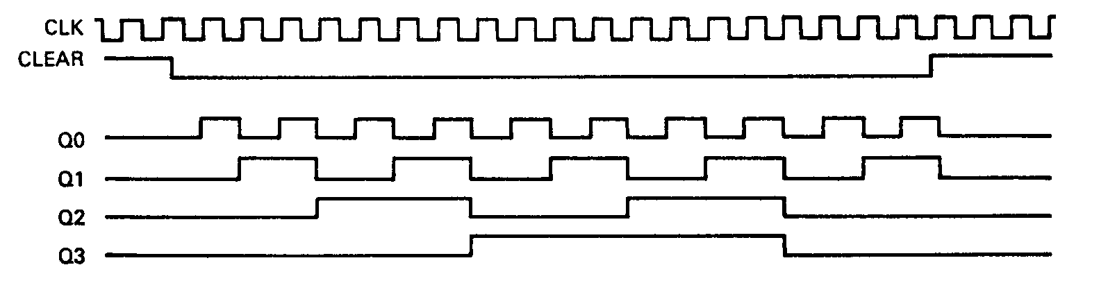
When the clock signal (pin 1) goes from low to high, the registers change state to reflect the new counter value, which then appears on the device outputs as logic level 1 for all outputs (corresponding to a counter value of 0). Since there is a delay between the time the new register values appear on the flip-flop outputs and the time these values propagate back through the programmable array, the counter's flip-flop inputs will require a certain amount of time to stabilize before being clocked again. This limits the speed at which this design can be operated. A timing diagram of the counter circuit is shown in figure 16. The diagram shows the relationship between the 16R4's clock input and the resulting counter values appearing on the counter's four outputs. To ensure that the counter can be initialized to a known value immediately after power-up, it has been provided with a synchronous clear input. When the clock signal (pin 1) goes from low to high, the registers change state to reflect the new counter value, which then appears on the device outputs as logic level 1 for all outputs (corresponding to a counter value of 0).
Since there is a delay between the time the new register values appear on the flip-flop outputs and the time these values propagate back through the programmable array, the counter's flip-flop inputs will require a certain amount of time to stabilize before being clocked again. This limits the speed at which this design can be operated. For most applications, though, the propagation times are short enough that this speed constraint is of little concern.
The 16R6 and 16R8 devices are identical to the 16R4, the only difference being in the number of registered outputs. The 16R6 has six registered outputs and two combinational outputs, while the 16R8 has eight registered outputs and no combinational outputs. Twenty-four-pin versions of these devices are also available (such as the 20R4, 20R6, and 20R8 devices) and are in all respects identical to the 20-pin devices with the addition of four extra input pins.
In recent years, configurable (sometimes called generic) device architectures have become extremely popular. These devices simplify procurement, qualification and inventory requirements by replacing a large number of simpler PAL type devices with a "one size fits all" device. In addition, their flexible architectures allow designs to be implemented that are challenging or simply impossible for the simpler PAL devices to handle.
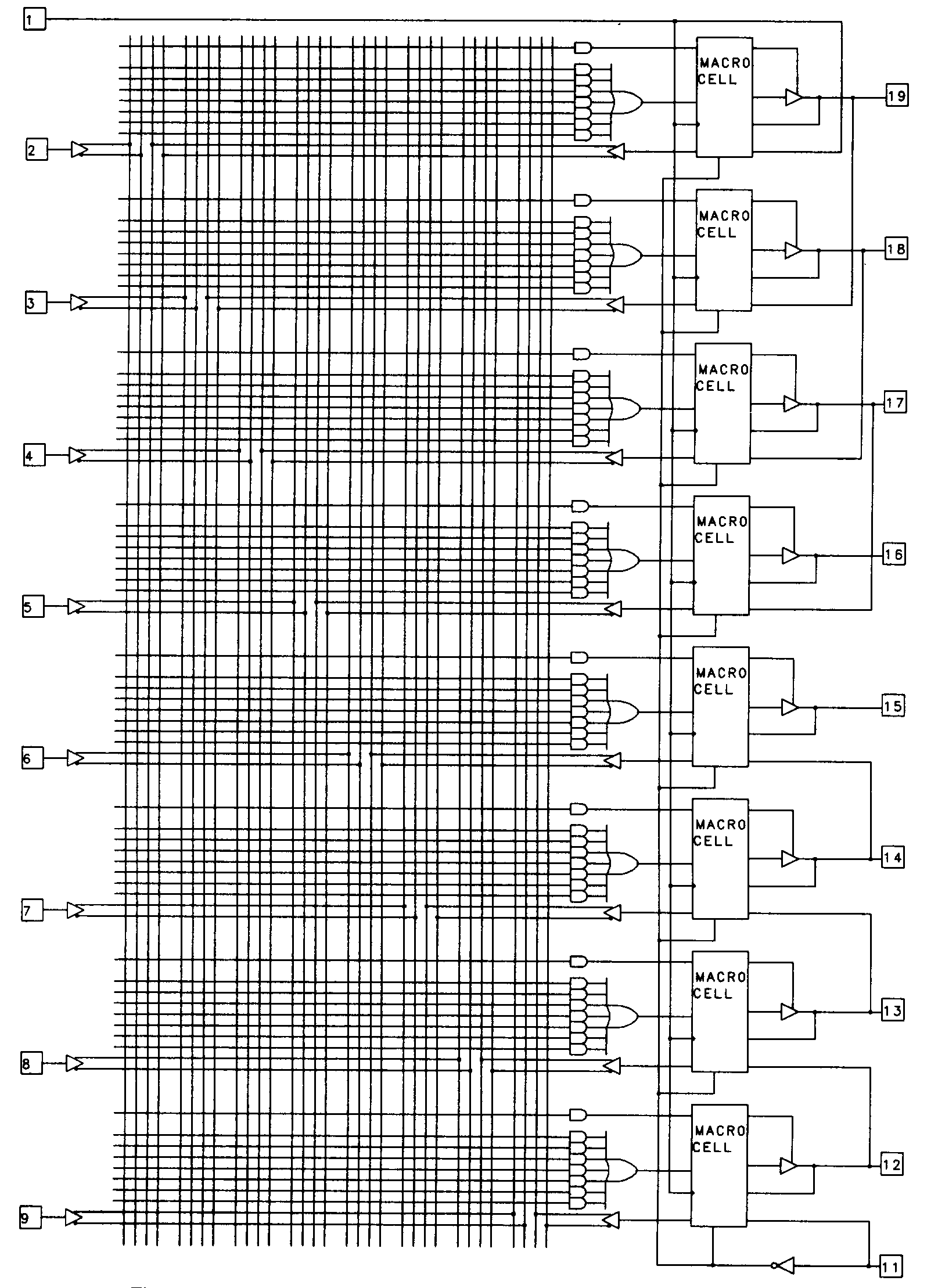
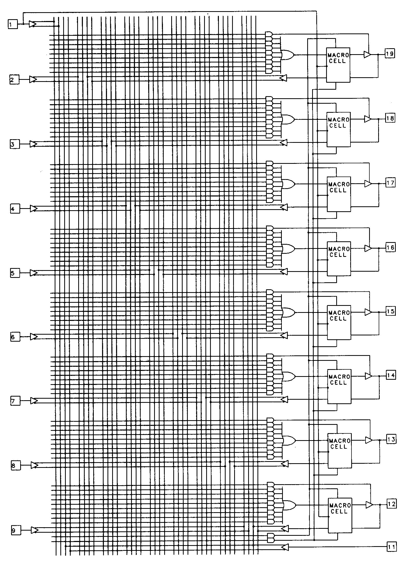
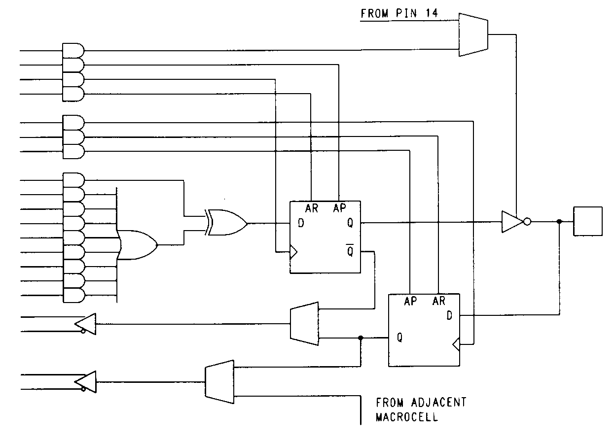
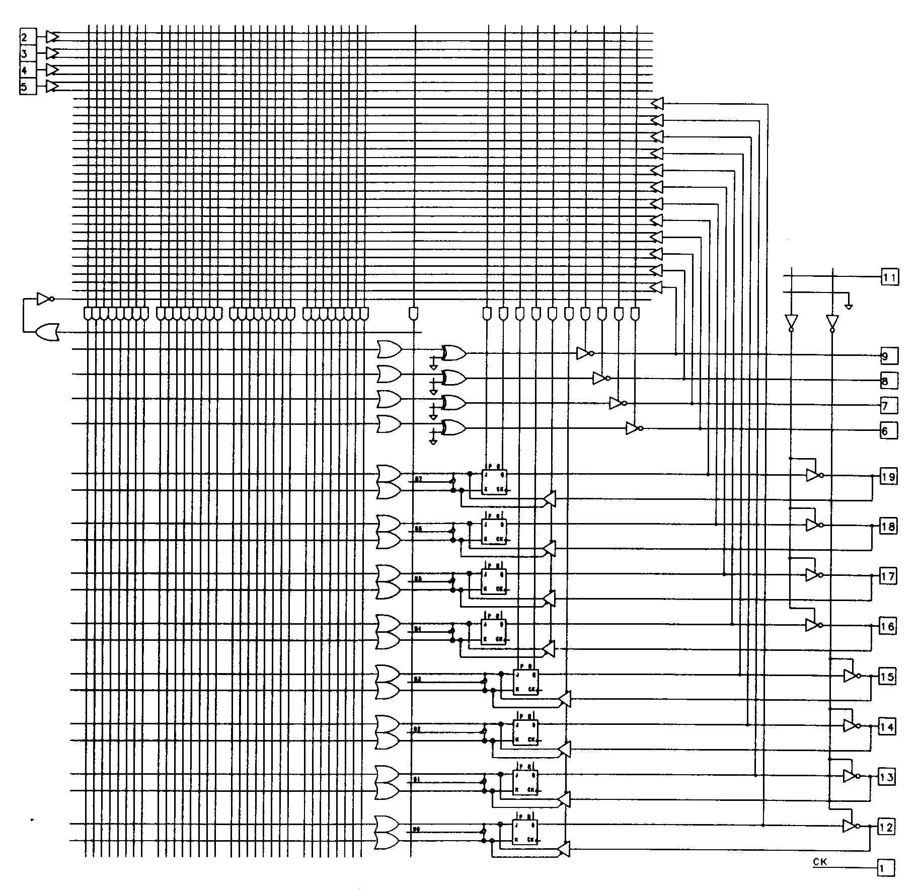
This architectural flexibility is provided by equipping the device with a variety of configuration fuses separate from those found in the programmable AND array. The 22V10 is one such device, and was designed by AMD to be a replacement for all of the 24-pin PALs of the architecture previously described. To meet this requirement, the 22V10 was designed with configurable outputs. These outputs are enhanced with special circuitry and are called output macrocells. Output macrocells are found on ten of the 22V10's pins, as shown in Figure 17.
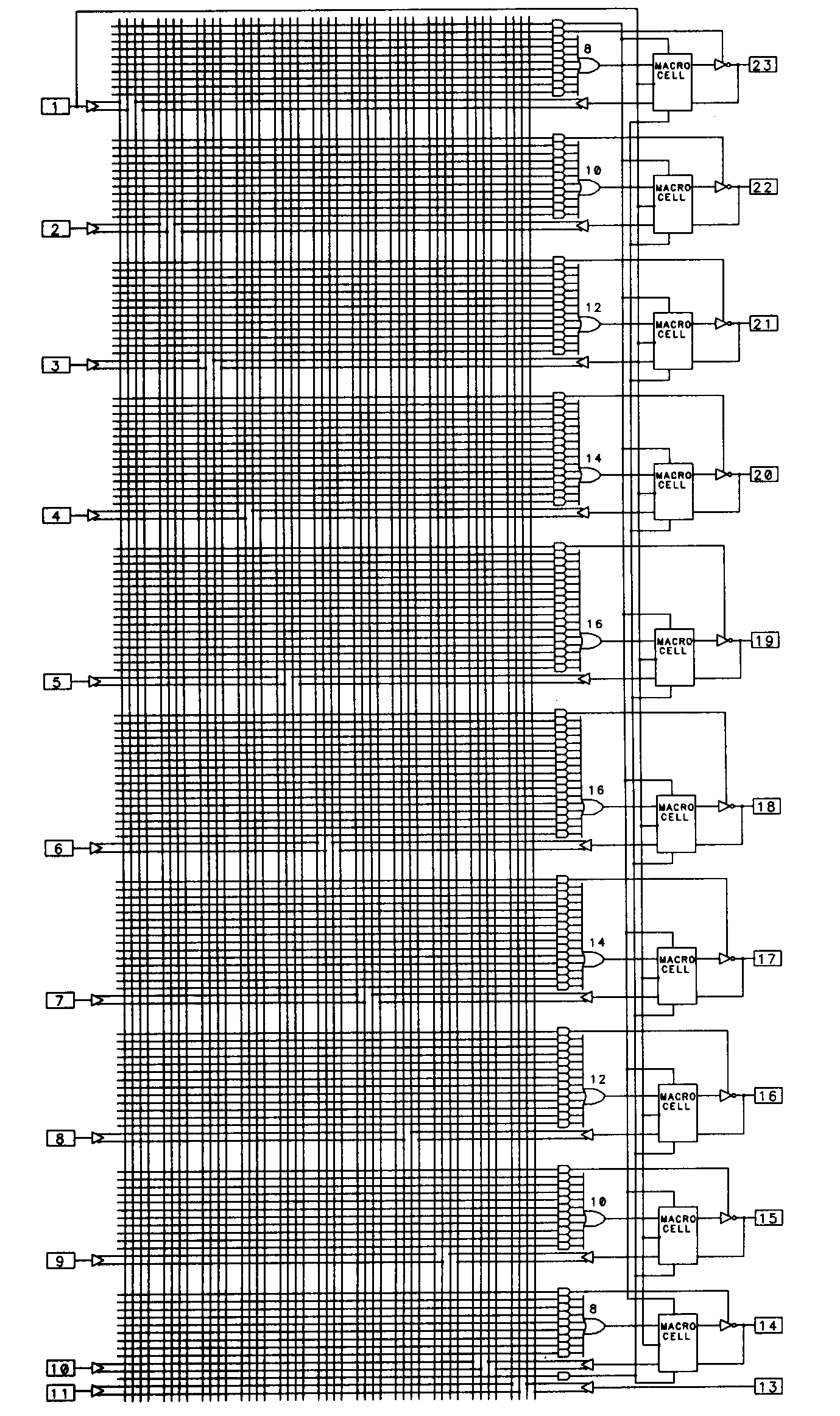
The 22V10 has a total of twelve dedicated inputs, one of which (pin 1) also functions as the common clock input to the edge-triggered D-type flip-flop of each output macrocell. Any of the 22V10's ten output pins can be used as inputs, so the device is capable of supporting applications requiring up to 22 inputs (of course, if you use all ten I/O pins as dedicated inputs, there is no way to observe the results of your efforts, since there will be no output pins left).
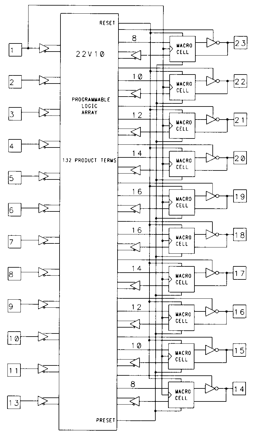
We will examine the structure of the individual output macrocells momentarily, but first, notice that the number of product terms available to the various OR gates in the device differs. The OR gate associated with pins 18 and 19, in fact, have sixteen product terms each available. This means that logic functions of significantly more complexity can be implemented in the 22V10. The irregular nature of the outputs does place more burden on the designer, though, since the design outputs may have to be assigned to device outputs based on their complexity. The complexity of the 22V10 results in a rather unwieldy logic diagram. For larger devices, the logic diagram format becomes completely impractical, so these devices are often presented in block diagram form. Figure 18 illustrates the 22V10 in block diagram form.
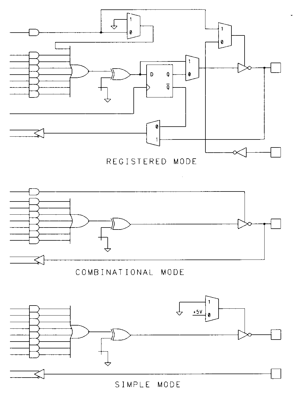
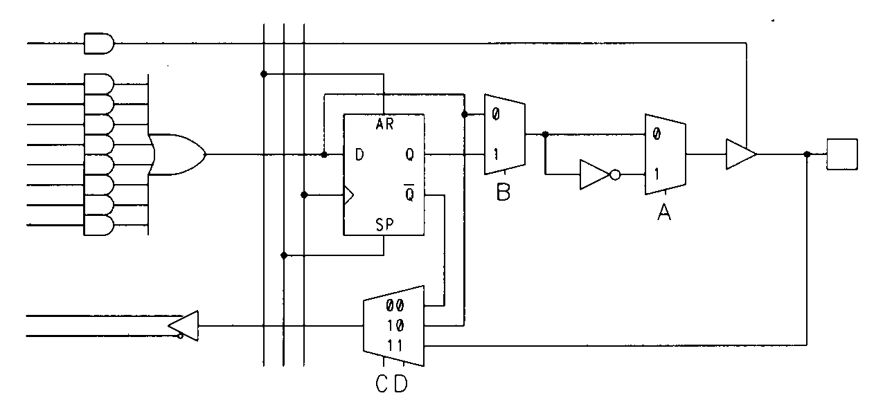
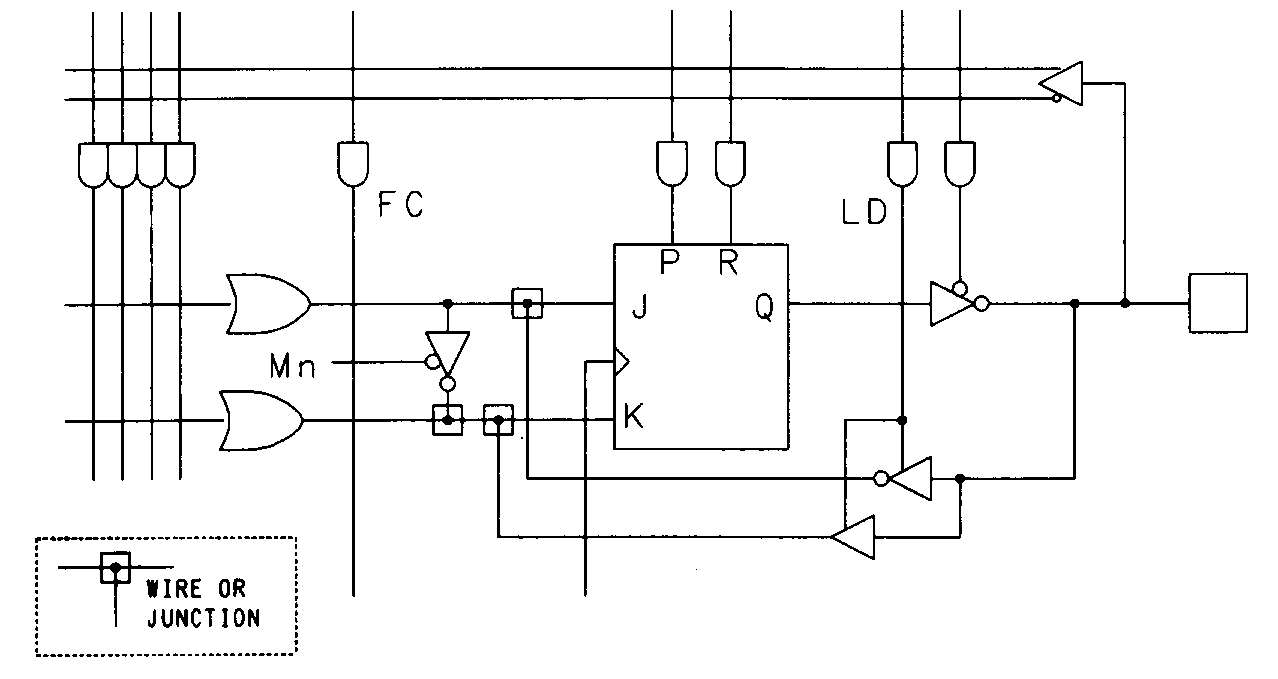
As I said, the 22V10 has ten output macrocells, all of which are identical. Figure 19 shows the construction of one of these output macrocells.
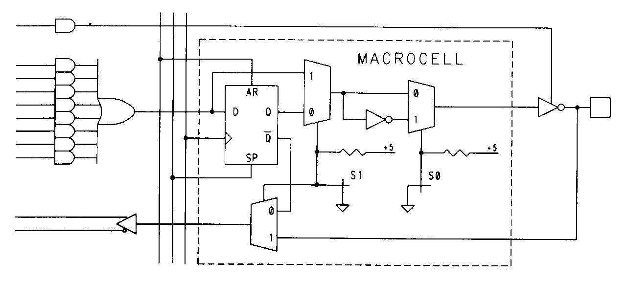
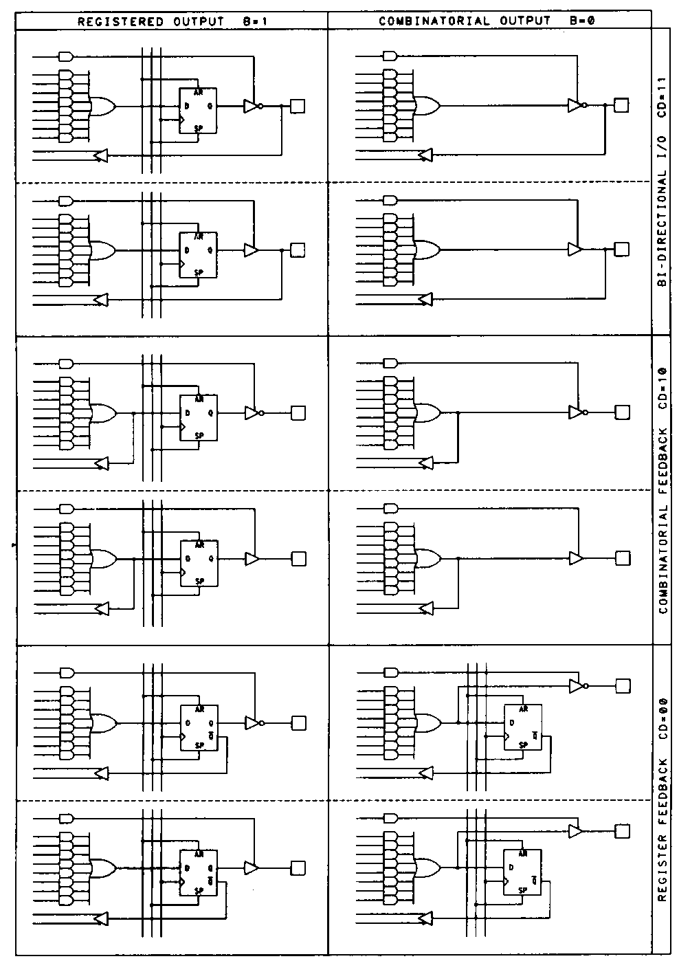
Each macrocell contains an edge-triggered D-type flip-flop and a pair of configurable multiplexers (I have shown the 22V10s configuration multiplexers complete with their fuse interconnections and pull-up resistors; in subsequent figures I shall omit the fuse and resistor). The two fuses that control the multiplexers can be configured in four different ways, as shown in Figure 20.
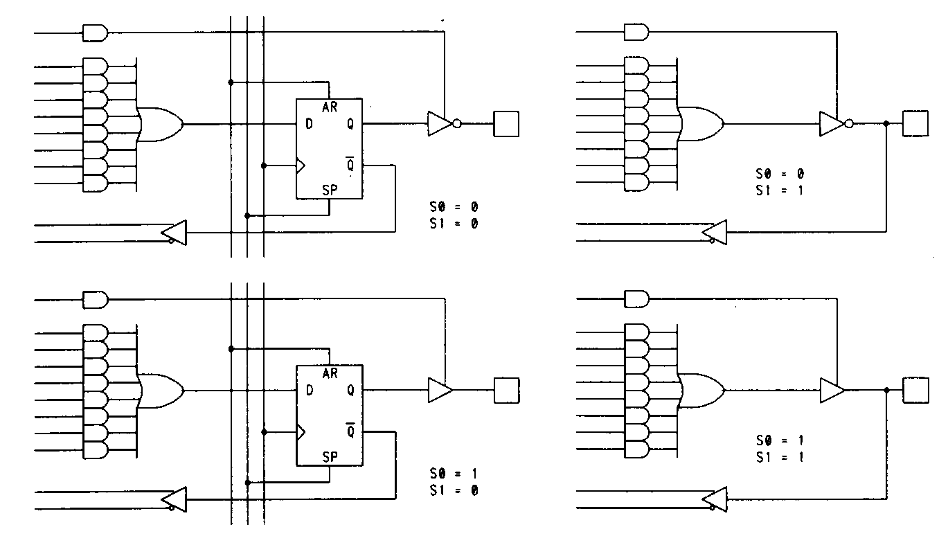
The 22V10 also has available two extra product terms that can be seen in Figure 17. These product terms can be used for synchronously presetting the 22V10 registers, or asynchronously resetting them. The feedback in the 22V10 can be configured to be from the register, the output pin, or from the OR gate output. While AMD's 22V10 has the feedback path and register bypass configurations controlled with a single fuse. TI's 22VP10, on the other hand, has independently configurable feedback and register bypass.
Another example of a configurable PAL is the Lattice GAL (generic array logic) device. These devices, more so even than the 22V10, are intended as pin-for-pin replacements for a wide variety of PAL devices. The GAL device, in fact, is designed to be compatible all the way to the fuse level-JEDEC format files for virtually any simpler PAL can be directly implemented in the GAL device.
Another major distinction between the GAL device and the original 22V10 is the fact that the GAL is electrically erasable (later CMOS versions of the 22V10 are available that are erasable). This makes the GAL particularly well suited for engineering prototype activities. The GAL comes in two basic versions. The GAL 16V8 device replaces most 20-pin PAL devices, while the 20V8 replaces most 24-pin PAL devices. The 16V8 device is shown in Figure 21.
Like the 22V10, the GAL devices utilize a configurable output macrocell. Although the function of the GAL macrocell is similar to the 22V10, the GAL macrocell differs from that of the 22Vl0 in a number of areas. The GAL macrocell (which Lattice refers to as an output logic macrocell, or OLMC) is shown in Figure 22.
The most important difference is that the OR gate is considered to be a part of the output macrocell. This is necessary because of the differing architectures of combinational and registered outputs in devices like the 16R4 described earlier. The control fuses for the GAL macrocells allow each macrocell to be configured in one of three basic configurations. These configurations correspond the various types of I/O configurations found in the PAL devices that the GAL is designed to replace.
In the registered PAL mode, each of the 16V8's eight outputs can be registered or combinational. Those outputs that are configured with registers have eight product terms and a fixed enable input (from pin 11), while those that are combinational have seven product terms with a term-controlled output enable. Clocking in this mode is from pin 1, which can not be used as an input to the logic array.
In the combinational mode, the clock and enable inputs (pins 1 and 11) are made available as array inputs. In this mode, output pins 12 and 19 are not available for use as inputs to the array. The combinational mode is intended for emulation of the 16L8-type combinational PALs.
In the GAL's third mode, there are eight product terms available to each of the eight outputs and no output enable feature is provided. This mode is intended for emulation of the simple PAL-type devices (14H4, for example) so as many as 16 inputs can be used with two outputs available (in this situation, the two outputs must be pins 15 and 16, since these pins be used as inputs in this mode). The original GAL devices did not have pin feedback available in this mode, but the newer 16V8A devices do support this feature.
Still another family of devices that are intended as PAL replacements are the PEEL devices from International CMOS Technology. The PEEL 18CV8, shown in Figure 23, features output macrocells that can be configured in any of twelve different ways.
The PEEL output macrocell is illustrated in figure 24.
The PEEL's macrocells provide a wider selection of feedback options than do the GAL's. Notice that there are four fuses used to select the macrocell configuration. Figure 25 shows the twelve different configurations possible for each macrocell using these fuses.
The PEEL's architecture supports the use of up to 18 inputs to the array (including feedback outputs); the clock and enable pins can be used as inputs to the array even while they are being used for their primary functions. The same architectural features with 22 inputs are provided in the PEEL 20CG10, 22CV10, and 22CVlOZ devices. Like the 22V10 device, the PEEL includes product-term controlled preset and reset functions. The 24-pin 22CVlOZ, in fact, can be used as a functional replacement for the 22V10. Like the GAL, the PEEL device is erasable through the use of CMOS EEPROM technology. (This technology will be discussed in more detail later.)
Exclusive-OR gates, or XORs, are found in PALs for a variety of purpose. (We have already seen how XORs are used to implement fuse configurable output polarity). XORs have other applications as well. Figure 26 is the logic diagram for the 20X8 device.
The device has an XOR feeding each of the device's flip-flops. Each of these XOR gates is fed in turn by two sum-of-products arrays of two product terms each. These XORs can be used to reduce the amount of logic required for many applications, particularly counters. The XORs not only allow dynamic polarity control of the outputs, but also allow surprisingly complex designs to be implemented using very few product terms. In recent years, the value of these extra gates has become increasingly apparent to circuit designers.
Independently clocked flip-flops are useful in many applications (such as synchronous state machine applications) and an increasing number of devices support this feature. The first device to have independently controlled clocks was MMI's 20RA10. The 20RA10's macrocell architecture is shown in Figure 27.
This 24-pin circuit features product terms that control each of the device's ten D-type flip-flops. The flip-flops also feature a transparent latch mode that is selected by asserting both the preset and reset signals high.
In the devices presented thus far, we've seen how configurable macrocells allow a single PAL type devise to replace a number of different types of fixed output PALs. We have also seen how the adding of various output macrocell features such as XORs have extended the capabilities of the standard PAL architecture. Configurable output macrocells can also be used to increase the effective size of a device.
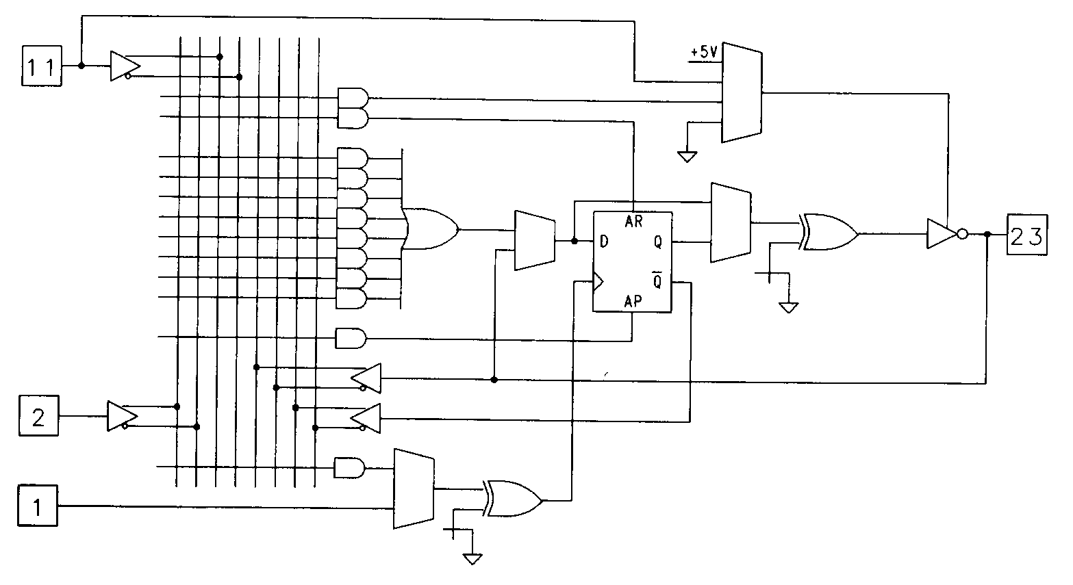
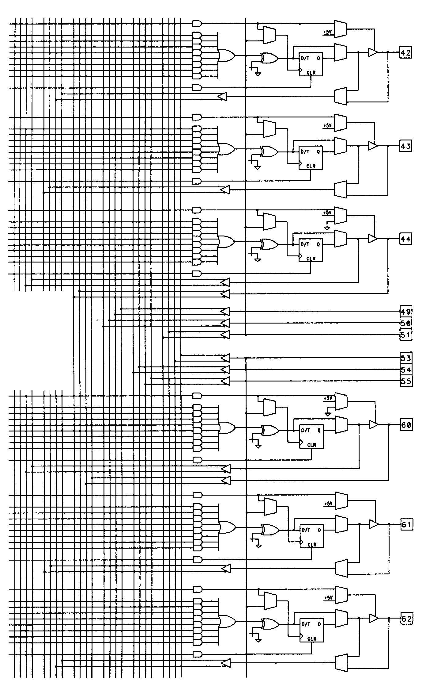
Examples of particularly powerful macrocells are found in the Altera EP600 and EP900 families of devices. The EP600 and EP900 families are popular UV-erasable devices of 24 and 40 pins (in DIP packages), respectively. Figure 28 illustrates the smaller EP600 device in block diagram form.
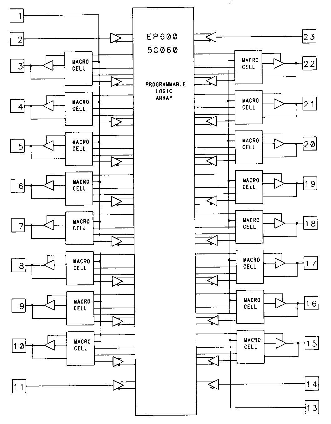
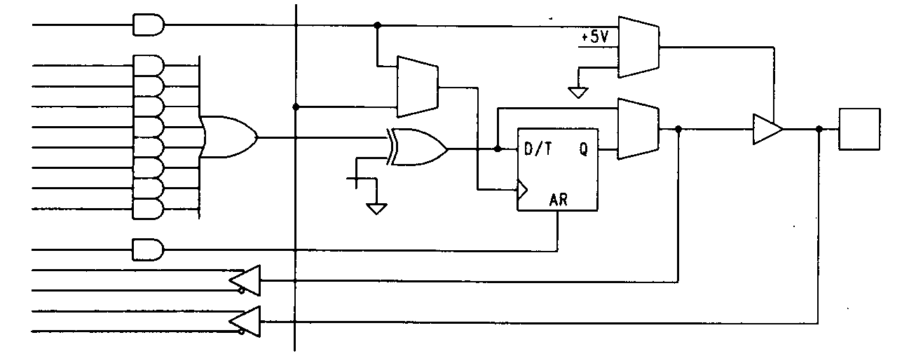
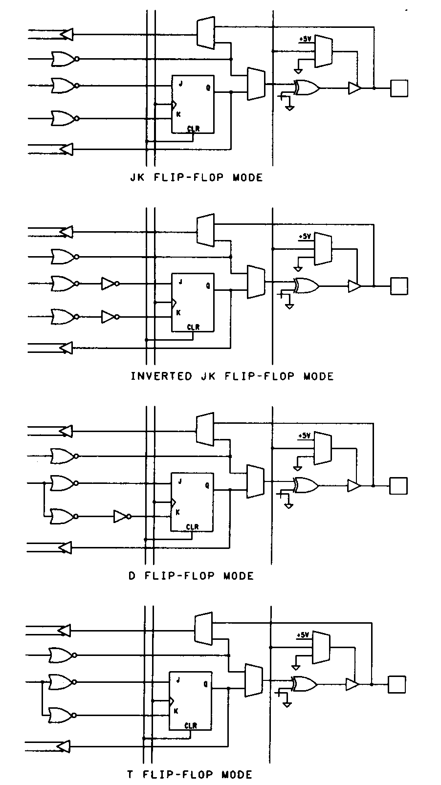
The macrocells found in these two families of devices are identical and have a number of useful features. As shown in Figure 29, the EP600 and EP900 macrocells feature the ability to be configured for operation as combinational inputs and/or outputs, or as configurable flip-flops that can be D-type or T-type. (JK-type or SR-type flip-flops can be emulated in the devices using Altera's design software.)
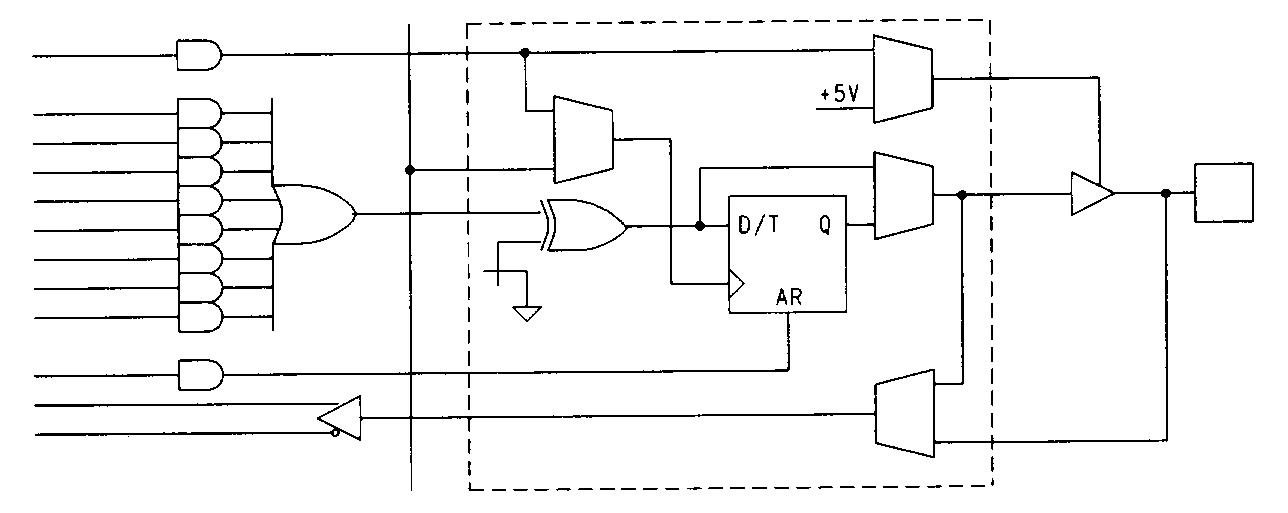
These devices were designed with high-level design tools in mind, so they are regular in their construction and highly configurable. The flip-flop emulation features are designed so that no product terms are wasted in the device when alternative (non D-type) flip-flop types are used. Programmable inversion is provided between the PAL array and the flip-flop inputs, simplifying the use of programmable polarity.
When operated in the D-type or T-type flip-flop mode, the feedback path from each macrocell can be configured to route the feedback from the flip-flop, route it from the associated I/O pin, or disable feedback entirely. When JK-type or SR-type flip-flops are emulated, feedback from the I/O pin is not available.
Asynchronous operation is provided by a clock-select multiplexer. The multiplexer for each macrocell is fed by a single product term that can be routed to either the associated flip-flop's clock input, or to the output enable for the associated device pin. When this product term is routed to the output enable, the flip-flop is clocked from a global clock pin; when the product term is used for clocking, the outputs are always enabled. The EP900 family of devices have two clock pins, each of which can control up to twelve of the EP900's 24 macrocells. The flip-flops in the EP600 devices are similarly banked, with a total of sixteen macrocells clocked from two dedicated pins. In addition to the clock/enable product term, another product term is dedicated to each macrocell for clearing the macrocell's flip-flop.
Another popular device that features complex macrocells with asynchronous capabilities is the AMD 29MA16. This device has sixteen complex macrocells (one of which is shown in Figure 30) that include configurable clock sources that can be either from a dedicated device pin or from a product term unique to each macrocell. Output enable is also selectable from multiple sources: either from a dedicated pin, from a product term, or fixed.
The 29MA16's registers are further configurable to operate as edge-triggered D-type flip-flops or as level sensitive latches. Dual register feedback provides the ability to bury the registers for state machine purposes while using the associated pin as an input. It's also possible to use the 29MA16's registers for input synchronization purposes by connecting the pin directly to the register's D input.
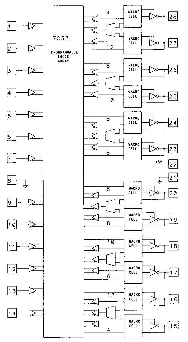
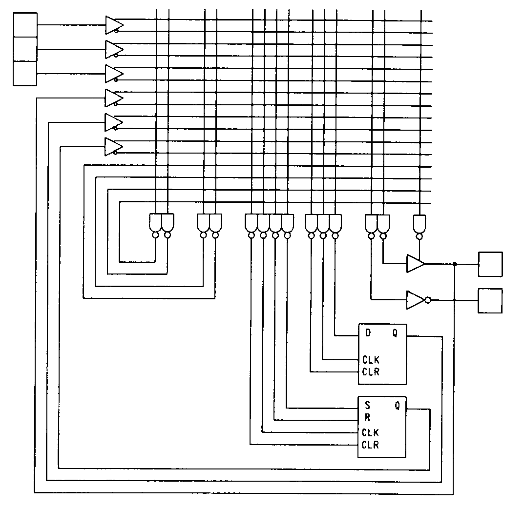
The trend toward more configurable output macrocells has continued to the point where the macrocells have grown so complex that it's almost impossible to comprehend them without the aid of software tools. One such complex macrocell is found in the Cypress 7C331. The device is shown in block diagram form in Figure 31. As the diagram shows, the macrocells are paired, and each pair of adjacent macrocells has a common feedback path, in addition to their own dedicated feedback paths.
The 7C331's macrocell architecture is shown in Figure 32. As the figure shows, the 7C331 has XOR gates associated with each macrocell. These XOR gates are arranged with one of their inputs fed by a single product term, while the other is fed by a normal sum-of-products array. The number of product terms allocated to each macrocell varies in the device -- a situation common in complex PALs. The asymmetrical XOR architecture makes it easy to emulate T-type or JK-type flip-flops in the 7C331.
In addition to the primary D-type flip-flop, a second flip-flop is associated with each of the 7C331's twelve output macrocells. These secondary flip-flops can be used as input registers while the primary flip-flops are being used as buried state registers. Both flip-flops can be bypassed dynamically by asserting their preset and reset signals simultaneously. Notice that the presets and resets of both the 7C331 and 29MA16 are asynchronous, unlike in the 22V10 where the preset is synchronous and reset is asynchronous. Having both the preset and reset asynchronous allows polarity reversal (often necessary to fit a design equation into the device) to be accommodated easily through the swapping of preset and reset functions.
An architectural tradeoff is found in the 7C331's dual feedback scheme. Rather than providing dual feedback paths for all macrocells, the device instead has feedback paths that are shared between pairs of adjacent macrocells. This means that buried state registers must be assigned to pins based on the availability of feedback. Cypress parts are known for their high-speed operation, and the 7C331 is no exception. The device is packaged in a large 28-pin DIP, but has dual ground pins to help reduce ground bounce problems.
The PLA was the basis for the first programmable logic devices. Devices that include a complete PLA (with programmable AND and OR arrays) are more flexible in terms of the variety of circuits that can be implemented in them. Their drawback is that they tend to be slower and more expensive due to the second programmable array.
One of the simplest examples of the PLA architecture is found in the Signetics PLS100. This device is diagrammed in Figure 33.
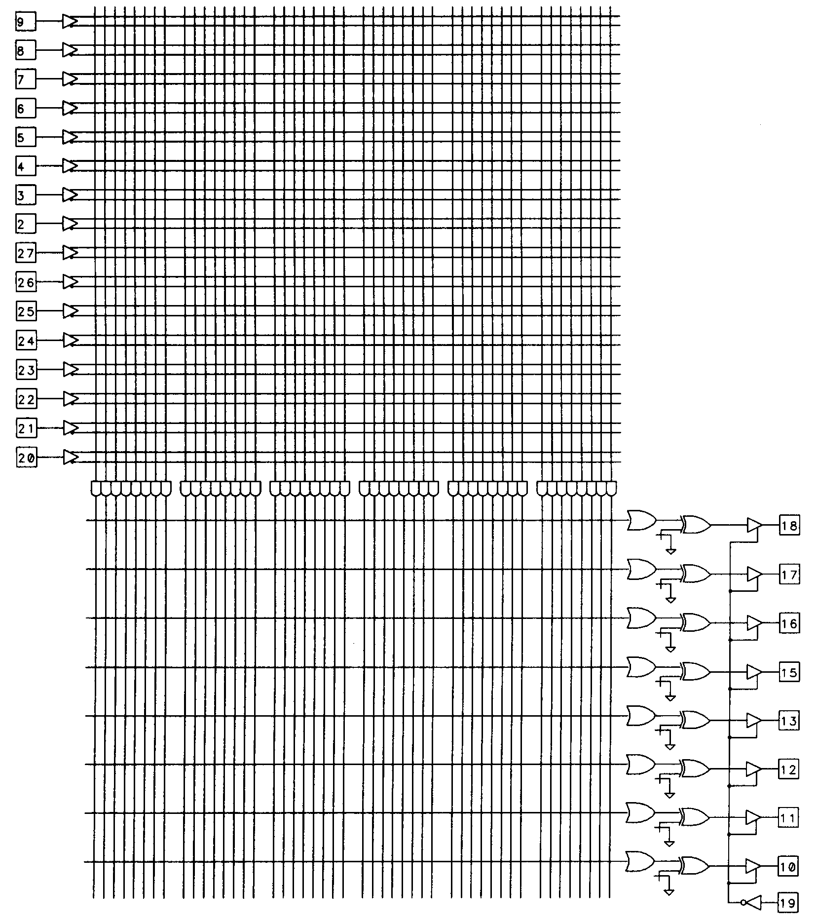
The diagram orientation commonly used for PLA architecture looks somewhat different from the PAL diagrams we have previously presented. The biggest difference is that the product terms are represented by vertical (rather than horizontal) lines. This representation makes it easier to illustrate the programmable OR array, which is the lower of the two arrays.
As Figure 33 shows, any of the 48 product terms for this device can be accessed by any OR gate. This makes it possible to implement more complex logic functions than possible in a PAL device of similar pin configuration. The device shown has no provision for configurable I/O, aside from the ability to select an output inverter for each output pin. A 24-pin version of the PLS100 device is available and is called the PLS161.
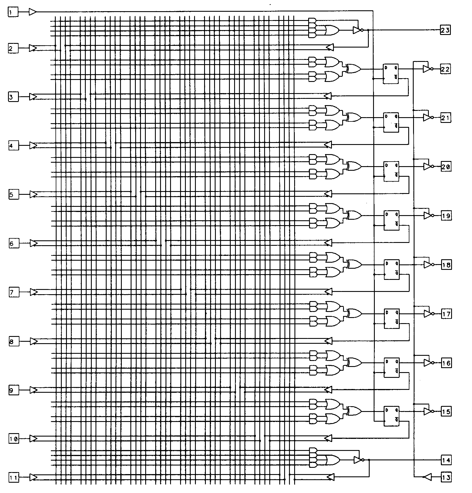
The most popular PLA-type devices are designed for state machine applications. The first of these, which Signetics refers to as FPLS type devices, was the Signetics 82S105, which is now called the PLS105. This device is shown in Figure 34. The PLS105 has a number of interesting features that set it apart from the registered PALs in its ability to implement complex state machines.
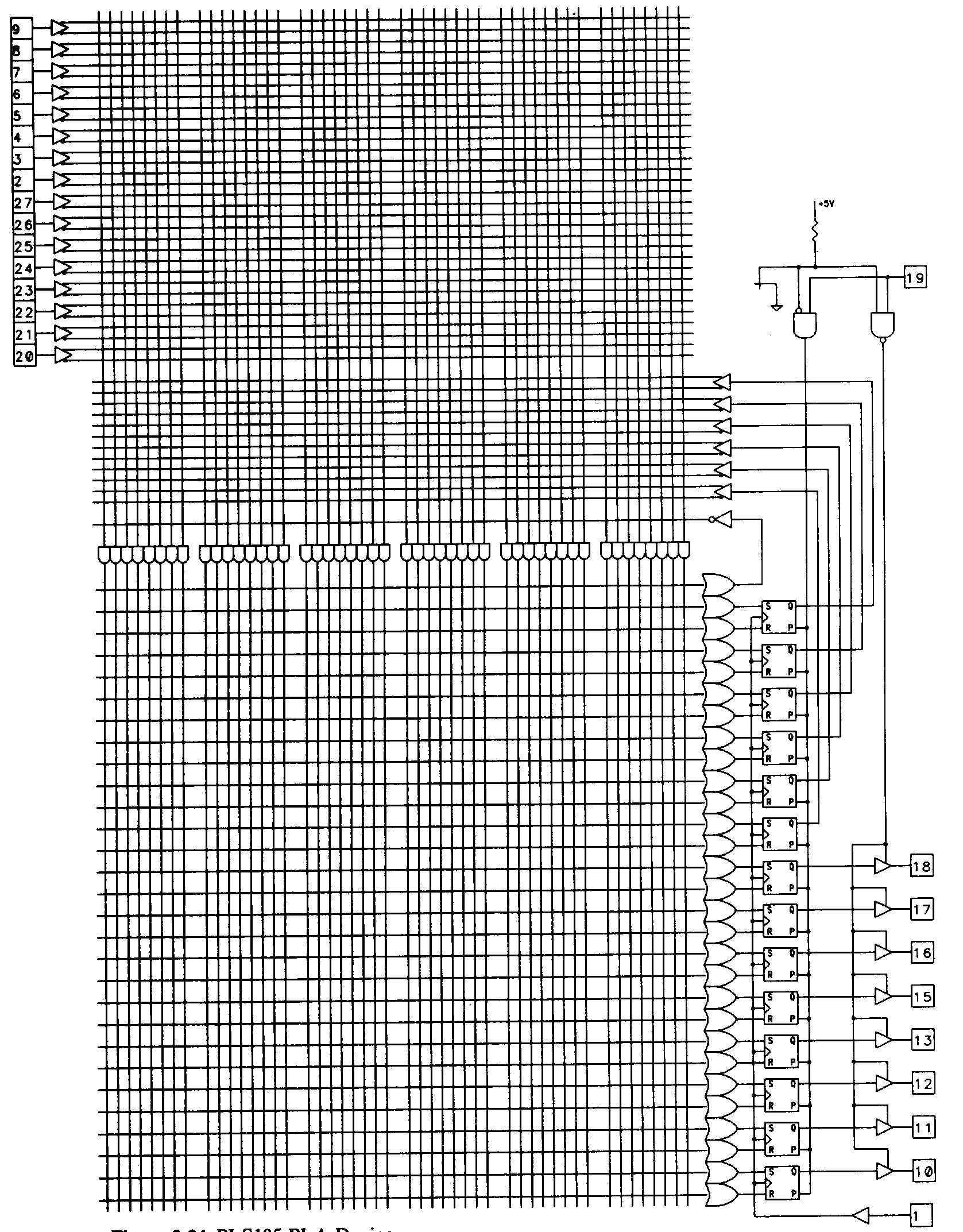
The first unique feature found in the PLS105 is its use of SR-type flip-flops for memory elements. SR-type flip-flops are particularly well suited to state machine applications, often requiring far less logic to implement transitions than equivalent designs implemented using D-type flip-flops.
Six of the PLS105's SR-type flip-flops are buried within the device, and aren't accessible as outputs. They are, however, fed back to the AND array. This buried register feature is being found on an increasing number of devices. The remaining eight SR-type flip-flops are associated with device outputs, and are not fed back to the AND array. This configuration of internal state memory and output synchronization registers is ideally suited to complex state machines.
Implementing complex state machines in PAL devices can be difficult because there are generally not enough flip-flops to provide both state memory and output synchronization. In a device such as the PLS105, however, such state machines are straightforward and easily achievable.
Another feature found in the PLS105 is the complement array. The complement array is a single OR array output that is inverted and fed back into the AND array to provide a very useful function, which is to detect undefined states and force the machine to return to a known state.
One attribute that limited the early success of the PLS105 is its size. The device has 28 pins, which is larger than the standard 20- or 24-pin PAL devices. In a DIP package, this device takes up quite a lot of board space. In the newer PLCC (plastic leaded chip carrier) packages, however, 28 pins is a more reasonable number, so this decade-old design is gaining in popularity. The PLS105 device does have a smaller brother, the PLS167, that is supplied in a more conventional 24-pin package with corresponding reductions in the number of available inputs and outputs while retaining the same number of buried state registers.
TI's TIBPLS506 and TIBPSG507 are similar in architecture to the Signetics PLS105, featuring SR-type flip-flops for internal state registers and for output purposes. The TIBPLS506 feature an increased number of buried registers over the PLS105 and also includes a complement array. Unlike the PLS105, the output registers in the TI devices can be bypassed for combinational uses.
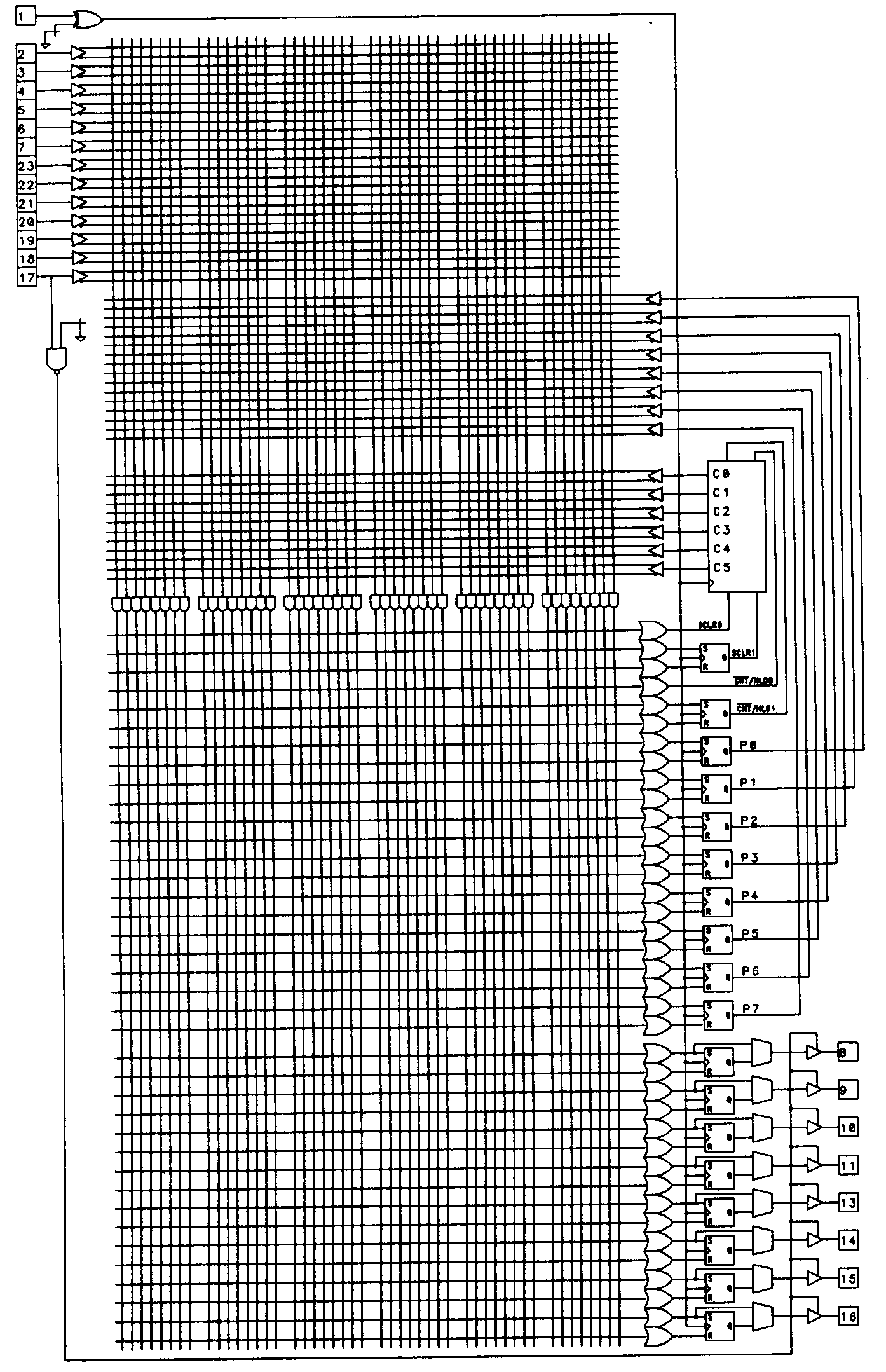
The TIBPSG507 is a specialized sequence generator device that includes an internal 6-bit counter. The device (diagrammed in Figure 35) is intended for applications such as waveform generators, dividers, timers, and counter-based state machines.
Another popular PLA-type device is the Signetics PLS159 device. This device, shown in Figure 36, extends the flexibility of the PLS105 architecture while at the same time reducing its size.
In the PLS159, there are eight registers, each of which can be used as either a state memory element or as a synchronized state machine output. In addition, four additional combinational l/O pins (of the sort found in the 16L8) are provided that can be used as inputs, outputs, or feedback to the AND array for multilevel logic purposes. These combinational I/O pins have fuse selectable inverters, further increasing their flexibility.
The registers used in the PLS159 are far more flexible than their counter-parts in the PLS105. Rather than being composed of SR-type flip-flops, the registers are constructed from JK-type flip-flops. The use of JK-type flip-flops, coupled with the mode control product term (Fc on the diagram) and individually selectable mode control lines for each flip-flop (MO through M7), allows each register element to be operated either as a fixed JK-type, fixed D-type, or dynamically selectable D/JK-type flip-flop. The dynamically configurable flip-flop is detailed in Figure 37.
The availability of dynamically selectable register types gives increased power to the state machine designer. For example, the D mode can be used to load specific states into the machine and the JK mode can be used during normal machine operation. Signetics' newer PLC42VA12 device also features dynamically configurable flip-flops that can be bypassed if necessary.
Additional device features that aid in state machine design (and testability) include product-term controlled preset and reset and product-term enabled load functions. Like the PLS 105, the PLS 159 includes a complement array for escaping from undefined states.
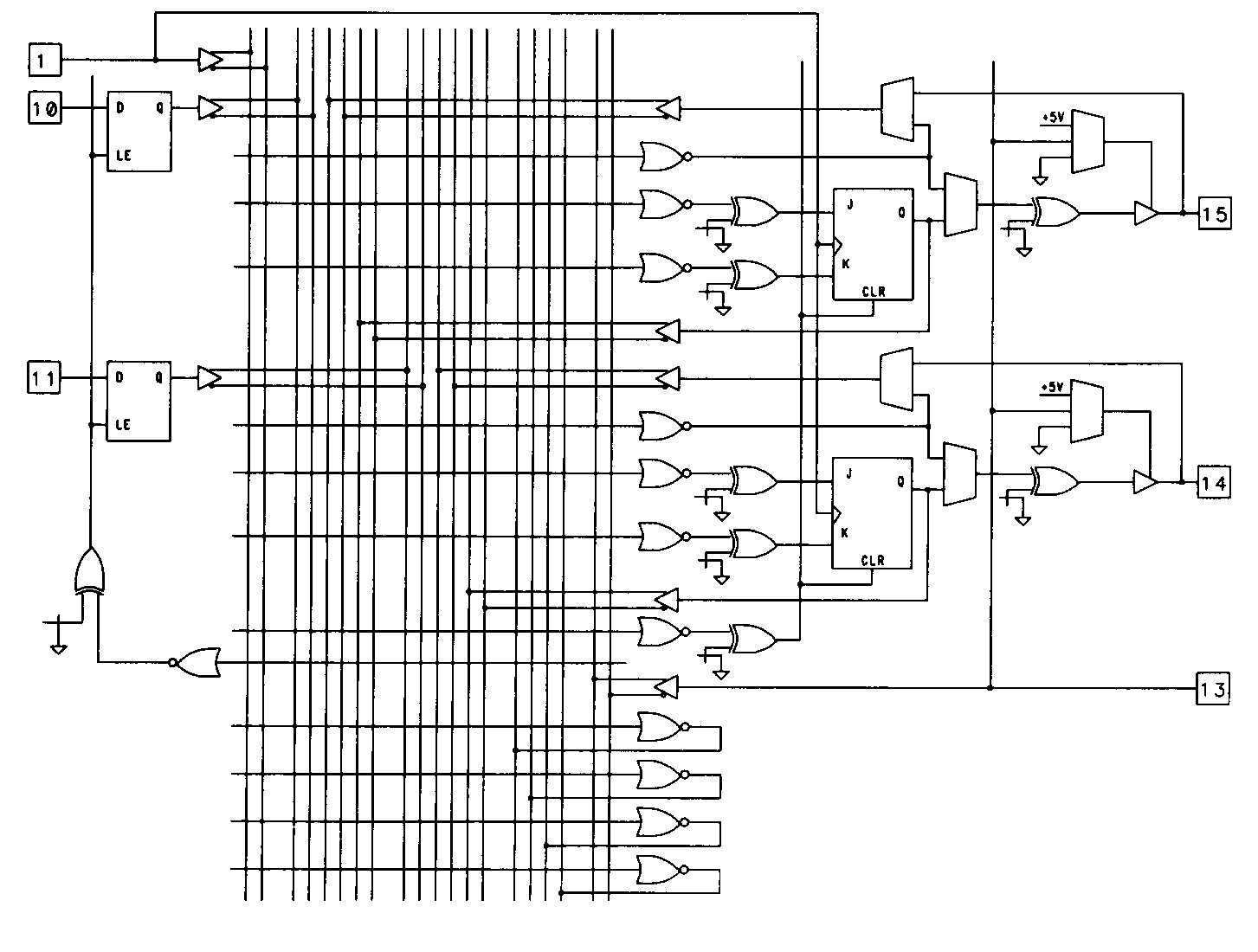
One of the most complex PLA-type devices currently available is the 6001 device from Lattice. This device also features configurable flip-flops and eight buried macrocells that can be used for state machine purposes. A simplified version of the device is shown in Figure 38 (the actual device has eight buried macrocells and ten I/O macrocells).
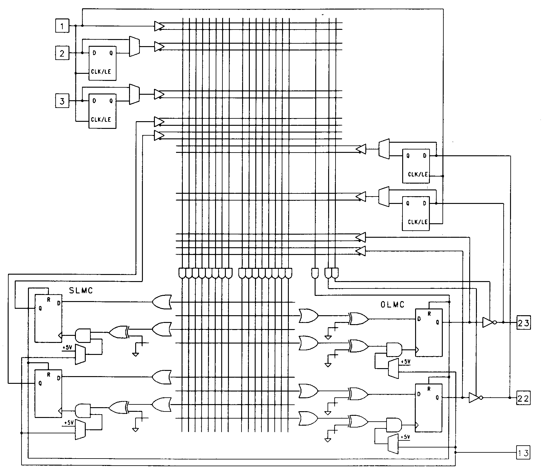
The device is significantly more complex than the earlier PLA-type devices. Not only does it have eighteen complex output macrocells, it has some other intriguing features. Before examining these additional features, let's look at the output macrocells.
Like the PLS105, the 6001 device has a set of buried macrocells. These eight macrocells are located on the left side of the diagram and are called the state logic macrocells, or SLMCs. The buried macrocells are identical in design and function to the ten output macrocells associated with pins 14 through 23.
Each of these eighteen macrocells is composed of a D-type flip-flop with gated clock. When operated in a D mode, the E input to the macrocell can be used as a clock enable line. This is useful for data latching and holding operations.
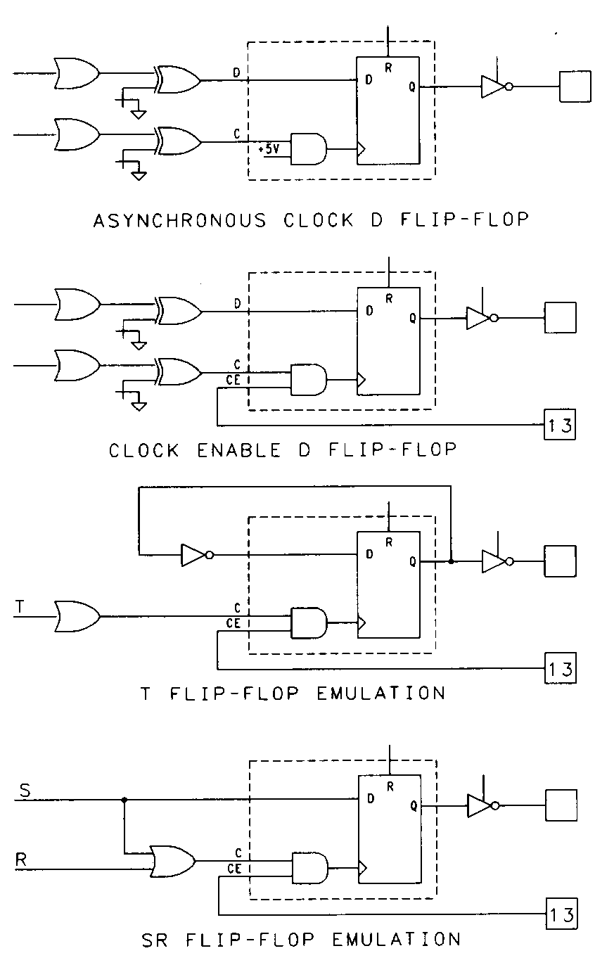
Alternatively, the E input to the macrocell can be used for asynchronous clocking purposes or for emulation of alternate flip-flop types, as shown in Figure 39. Notice that, since the 6001 is a PLA, it's possible to emulate SR-type flip-flops with no waste of product terms.
As is the case in the 22V10 output macrocell, any of the 6001's flip-flops can be bypassed to provide purely combinational operation. Unlike most devices, it's possible to isolate any of the output macrocells from their associated output pins. This allows macrocells to be used as buried registers while at the same time using the corresponding pins as dedicated inputs.
The final feature that is noteworthy about this device is its set of banked input macrocells. These configurable macrocells are provided for all of the 6001's input and I/O pins, with the exception of pin 1. Each of the two input macrocell sections are configurable as a group to operate as either asynchronous, latched, or registered inputs. Configurable input macrocells such as these are appearing on more devices, and are useful for a variety of applications requiring input synchronization.
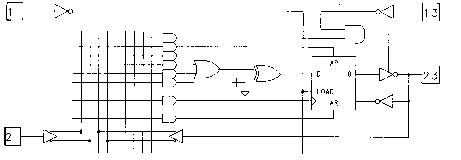
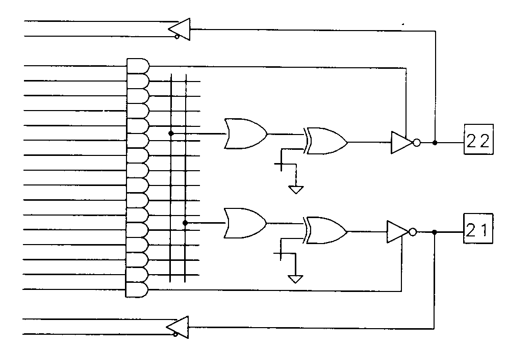
Product-term steering is a limited implementation of the PLA concept in a PAL type device. In its simplest form, a product-term steering device such as a 20S10 (shown in Figure 40) allows adjacent outputs to share terms. This means that those outputs provided with term steering can use as many as fourteen product terms each. This feature might be more appropriately called product-term stealing, since it isn't possible for both of the adjacent outputs to use the same product term.
Another form of product-term steering is found in the Atmel 750 and 2500 devices These devices feature buried macrocells associated with output macrocells. Figure 41 shows one output macrocell for the 24-pin Atmel 750 with its associated buried node.
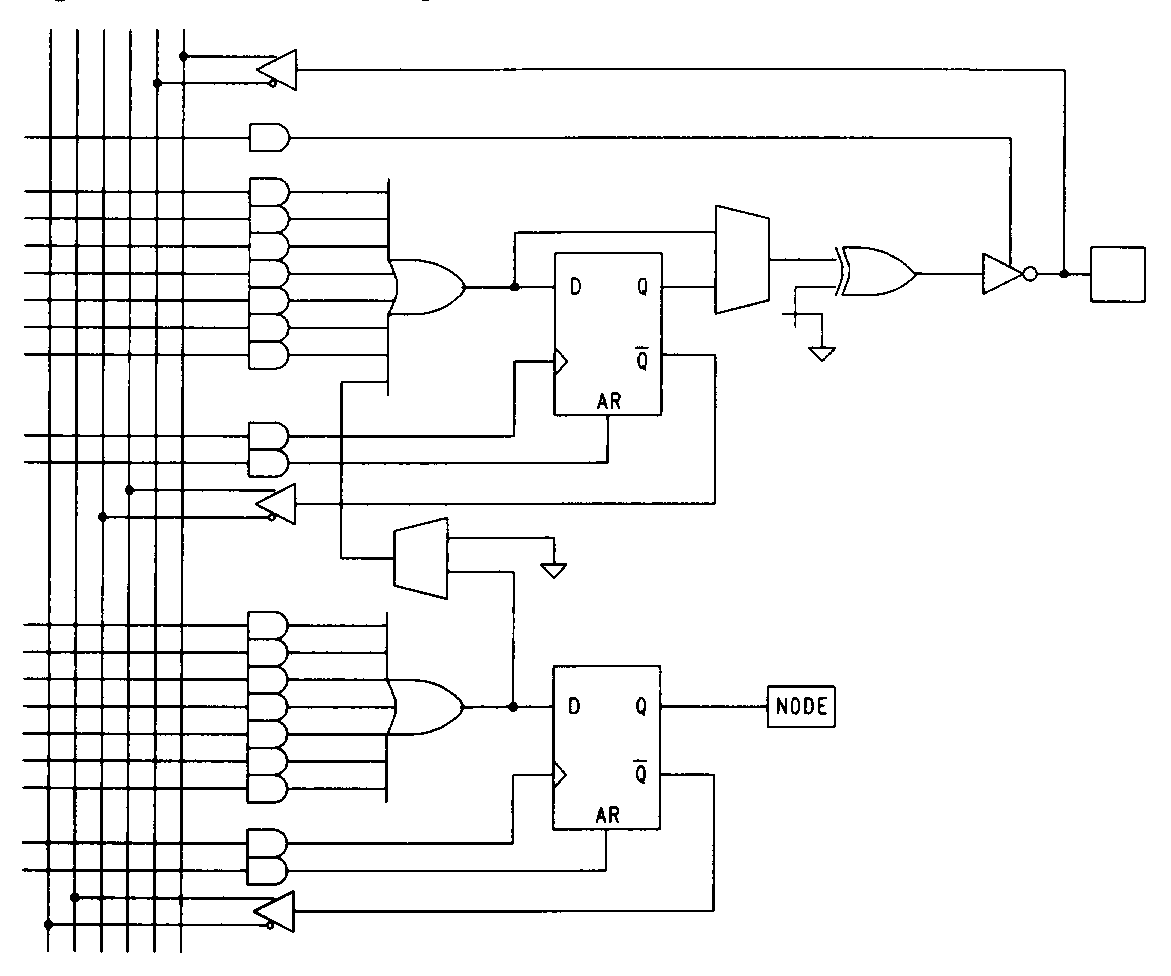
Typically, the buried macrocells are used for state registers but, if desired, the product terms feeding a buried node can be appended to the product terms of its primary macrocell. This effectively doubles the number of product terms available to the primary macrocell. The buried macrocell can still be used, assuming the shared product terms are appropriate for both functions. Figure 42 5AC312 product-term distribution The 40-pin Atmel 2500 device is similar, but features two buried macrocells for every primary macrocell.
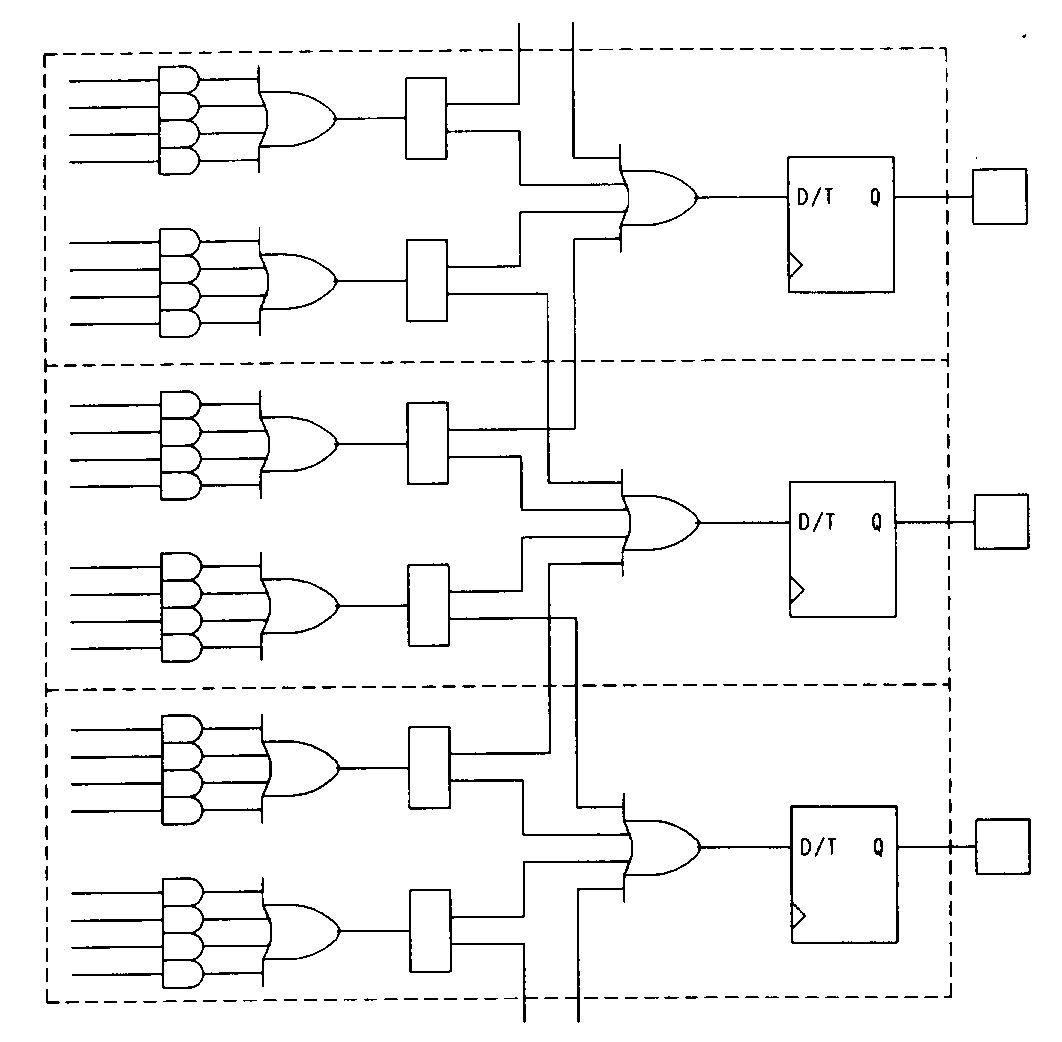
The Intel SAC312 has another form of product-term steering. As shown in Figure 42, the device has its product terms segmented into groups of four. These groups are each allocated to a single output of the device, but if more product terms are required for a particular output, they can be reallocated. The reallocation is limited to nearby outputs, allowing one macrocell to have as many as sixteen product terms.
Still another product-term steering concept is found in the Altera MAX family of parts. These devices include a set of product terms that aren't allocated to any particular output. These product terms, referred to as expander terms, can be allocated as needed to outputs that require additional product terms. Use of expander terms has speed penalties, however, so their use must be weighed against the performance criteria for the design. Figure 43 illustrates the expander term concept.
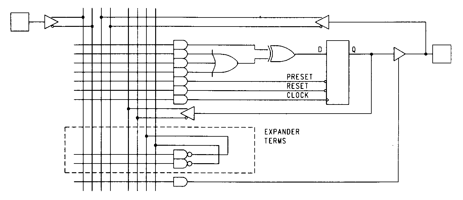
Unlike other term steering schemes, the expander term architecture requires that the design equations be converted into an alternate (non sum-of-products) form.
As PLDs increase in complexity, the size of the programmable array quickly becomes unmanageable. For this reason, some manufacturers have developed architectures that are segmented into smaller arrays with limited interconnections. One such device is the Altera EP1800 (shown partially in Figure 44).
The EP1800's programmable array is split into four identical quadrants that have limited interconnects. Portions of two quadrants are shown in the figure. This segmentation means that designs being implemented in the EP1800 must be partitioned and allocated to quadrants based on the amount of interconnection required. There are two types of feedback available in the EP1800: one feedback path is available to the local quadrant only, while the other path feeds signals globally around the device. This is illustrated in the diagram of Figure 45 which shows one output macrocell of the EP1800. The EP1800 macrocell architecture is identical to that of the EP600 and EP900 devices with the addition of the global feedback line on some (but not all) of the macrocells.
The EP1800 has some other interesting features, as well. The registers are configurable and may be used as T-type or D-type flip-flops. The clocking and output enable scheme is also interesting and allows either the clock or enable signal (but not both) to be controlled from a product term.
The sum-of-products array is, as we have seen, the mainstay of traditional PLDs. For large designs, however, the standard sum-of-products array can prove to be too restrictive. In particular, multilevel logic applications are difficult to implement in standard PLDs. To implement such designs in a PLD, succeeding logic levels must be fed back into the logic array, with often unacceptable speed penalties or wasted device resources.
One architecture that is better suited to such multilevel applications is the folded-NOR architecture pictured in Figure 46. The folded-NOR array permits successive levels of NOR gates to be fed back and cascaded to implement multilevel logic designs. The array shown is a simplified version of Exel's ERASIC device.
The ERASIC is a good example of a folded-NOR PLA device. The XL78C800 features ten highly configurable output macrocells and eight dedicated input latches in addition to the folded-NOR array. The device consists of a single programmable NOR plane, which can be used to generate logic of as many levels as logic for a single output as you would ever practically require. The only limitation is the number of NOR terms provided in the array.
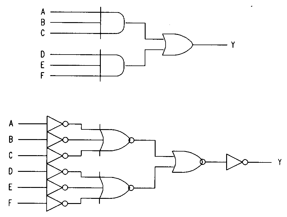
How does this work? Consider the logic shown in Figure 47. As the figure illustrates, it's possible to implement either a product term (an AND operation) or a sum term (an OR operation) in a NOR term simply by choosing the appropriate polarity of inputs to the NOR gate. (deMorgan?)
From this, it can be shown that all possible logic functions can be implemented in NOR-NOR logic, just as they can be implemented in sum-of-products. Furthermore, the use of just one array allows the implementation of multi-level logic functions that are quite cumbersome and wasteful to implement in a sum-of-products array.
The folded-back NOR terms are referred to as asynchronous feedback terms. In the ERASIC device, there are two types of these terms available. The lower part of the array (shown in the logic diagram) is composed of these terms in their simplest form. These 32 terms are not associated with any device output and so, are roughly analogous to the AND terms in a standard PLA (remember, however, that these NOR terms can be used for OR functions in a multilevel application).
The upper, more complex part of the array is broken into groups of NOR terms that feed the ERASIC's ten complex output macrocells. Each macrocell is fed by three NOR terms. In addition to the NOR terms associated with output macrocell functions, there are two additional NOR terms that are used for asynchronously clearing the device's flip-flops.
The different configurations of this output macrocell are shown in Figure 48. Notice that it's possible to bury the JK-type flip-flop and free the associated output pin for use as an input. It's also possible to bury the combinational NOR gate and feed it back to the array as an asynchronous feedback term while still using the pin as an independent output.
An interesting feature of this macrocell is the method used to control the output polarity. Rather than having an XOR gate on the register output, this macrocell contains programmable polarity elements on the J and K inputs to the registers. In order to reverse the polarity of the macrocell output, you must swap the J and K inputs. In this situation, the register clear function becomes a register preset. Using the programmable polarity flip-flop inputs, the macrocell can be set up to emulate D-type or T-type flip-flops by supplying either the D and ¬D inputs to the J and K inputs or by supplying the T inputs to both flip-flop inputs with no inversion.
Finally, the ERASIC device features latchable inputs on eight of the dedicated input pins. The latching of these inputs is controlled by two dedicated NOR terms.
Another family of folded-PLA devices is produced by Signetics. These devices, which Signetics has dubbed PML (Programmable Multilevel Logic) devices, feature a folded-NAND array rather than a folded-NOR array. A simplified diagram of the PLHS502 is shown in Figure 49.
The 52-pin PLHS502 (and it's smaller brother the PLHS501) have a large number of buried logic elements. As the diagram shows, the device includes eight SR-type flip-flops intended for state machine applications, and eight D-type flip-flops useful for shifter or output synchronization purposes. In addition to the folded-NAND array structure, the PMLs have a powerful clocking array (not shown) that allows many different clocking strategies to be used.
The versatility of the PAL architecture has led to a number of highly specialized programmable devices that are PAL-based. These devices are, by their very nature, difficult to categorize.
In-circuit reprogrammable PLDs are those can be reconfigured dynamically while they are operating in a system. One such device is the Lattice ISPGAL (In-System Programmable GAL). The 16Z8 ISPGAL is an in-system programmable version of the 16V8 GAL device. The 16Z8 has four extra pins that are used exclusively for programming operations. Having these extra pins means that the normal inputs and outputs of the device aren't interfered with during programming operations.
Asynchronous applications have long been a source of trouble for designers using PLDs, and device manufacturers have responded by introducing PLDs with more flexible clocking schemes, or completely asynchronous output registers. The 20RA10 and 29MA16 are examples of devices designed for asynchronously clocked applications.
The problem of metastability has led to some new PLD architectures intended for asynchronous interface applications. One such device is the PAL 22IP6 produced by AMD. This device utilizes unusual output macrocells that include non-clocked output registers, three of which are SR-type flip-flops, while the other three are dual T-type flip-flops.
These output macrocells, which AMD refers to as interface protocol asynchronous cells (IPACs) aren't subject to the risks of clock setup and hold violations, although the input signals applied to the IPAC registers must still meet certain, less stringent timing requirements.
Programmable bus interface devices fill a specific need for interface logic in bus-oriented systems. These devices are usually designed with a particular bus architecture in mind, such as the VMEbus or Micro Channel. Bus interface PLDs can be used to eliminate a large number of simpler devices normally required for such applications. Altera's BUSTER is one device that is designed for bus interface applications. The device has input synchronization registers, latched outputs, and a large number of configurable macrocells which are found both on I/O pins and buried within the device.
Another PLD intended for bus interface applications is the Intel 85C960. This programmable bus control is targeted specifically at systems utilizing Intel's 80960 microprocessors. The device provides address decoding, wait state, and ready generation at the relatively high speeds typical of systems using the 80960.
Intel also has a more general bus interface PAL called the BIC device. The SCBIC contains three octal latched transceivers that can be clocked in any of eight modes. Each I/O pin on the SCBIC has a configurable bus-oriented macrocell. In addition, the SCBIC has four buried macrocells.
PLX Technology has yet another of these devices. The PLX448 is similar to a 22V10 in construction, being based on the PAL structure. The device features ten inputs and eight bidirectional outputs. The PLX448's I/O drivers are compatible with the IEEE-448 interface standards possessing four outputs that can drive 48 mA loads, and four separately clocked outputs capable of driving 24 mA loads. Four of the outputs can be configured as open-collector type buffers. The PLX464 is similar and has outputs with 64 mA drive capability.
Programmable sequencers are hybrid devices that contain both a PAL array (used for state machine branch control) and a PROM-based microsequencer. MMI's PROSE device was one of the earliest of these devices and contains a bipolar PAL array (similar to the 14H2 PAL) of sixteen product terms along with a 128 word by 21-bit PROM array. Eight of the PROM outputs are connected to registered outputs, five are routed back into the PROM array, two are XORed with the two PAL outputs, and six are routed back into the PAL array as inputs. The PROSE device hasn't proven to be a popular part, partly because of the difficulty in using it (there is no high-level design tool support) and because of the limited advantages of using the PROSE versus implementing the same function in multiple smaller devices.
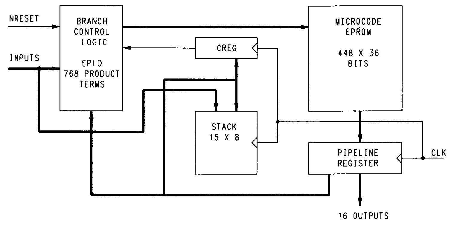
The Altera SAM device has had more success than the PROSE. This device is block diagrammed in Figure 50. The SAM is much larger than the PROSE, featuring a 768 product-term erasable PAL array and a 448-word by 36-bit EPROM. The SAM also features a 15-byte stack and an 8-bit loop counter. High-level design tool support is provided by Altera in the form of a microcode assembler and functional simulator.
AMD's 29PL141, like the Altera SAM device, is a microprogrammed device. Microinstructions are programmed into the chip's program memory. AMD's device has 29 microinstructions that include branching, subroutine calls, loops, and jumps. The device supports up to 64 states for state machine designs. Output data is stored in the device's PROM section. A block diagram of the 29PL141 is shown in Figure 51.
The AMD 29PL141 is supported with a microcode assembler that allows instructions to be written in a high-level language. These instructions are assembled into PROM data and microinstructions. Like a conventional PLD, the device uses JEDEC format files for fuse data and is programmed on a standard device programmer.
The high clock speeds of many modern systems place heavy demands on the speed of the interface logic for those systems, much of which can be most efficiently implemented in PLDs. There are two approaches to speeding up PLDs. The traditional approach has been to use high-speed technologies (processes) such as ECL (emitter control logic). This is expensive and creates interface problems when the PLDs must be integrated with the rest of the circuit.
A second approach is to modify the architecture of the traditional PLD, optimizing it for high-speed operations. This architectural approach to high-speed devices is seen in the Intel 85C508. This device is intended specifically for high-speed address decoder applications in which OR gates may not be required. The AND gates of this device directly feed its latched outputs, eliminating the propagation delay normally associated with the OR gate.
Another device which uses an architectural approach to high-speed circuits is the Cypress CY7C361. This device is quite complex and is optimized for high-speed state machine applications. The CY7C361 has a bank of 32 state registers that are located between the AND and OR arrays in a structure that Cypress calls a split-plane logic array.
The central location of the CY7C361's registers means that signals can propagate from the device inputs to the state registers with less gate delay than in traditional PLDs. More significantly, the delay times of the clock and register inputs are more closely matched, and the OR array outputs are synchronized through the use of a special de-skewing buffer. This combination of features allows the device to be operated at very high clock speeds.
An important architectural feature that is found on virtually all PLDs is not shown on logic diagrams. This feature is the security fuse. Normally, the fuse pattern programmed into a PLD can, like a PROM, be read and displayed or copied by programming hardware. Devices with a security fuse, however, provide the ability to disable this read function. This allows the design to be somewhat secure from attempts to copy or reverse engineer it.
In reality, it's relatively easy to shave the top off of a bipolar PLD and examine the programmed fuses with a microscope. For bipolar PLDs, then, would be copiers are merely inconvenienced. Erasable CMOS PLDs are considerably more secure, since it's very difficult, if not impossible, to determine their function from examination.
Many devices feature additional fuses that can be used to select operating modes appropriate for the requirements of the circuit as a whole. For example, the Altera devices feature a set of configuration fuses that allow control of their autonomous power-down features. Disabling the low standby power results in a higher usage of power and a higher speed of operation.
The ICT 22CVlOZ also features a power selection feature. Selecting the zero-power option for the 22CVlOZ results in a zero standby current mode and correspondingly slower device operation.
The device features we have seen up to this point have been primarily architectural features. As I stated earlier, there are some 300 different PLD architectures in existence. For any given architecture, however, there are possibly dozens (in some cases, even hundreds) of technologically different devices you can buy from one of many separate manufacturers. The devices you can buy will differ in many technology criteria. This section will cover some of these technology differences.
The two dominant processing technologies found in PLD manufacturing are bipolar and CMOS. Bipolar devices have historically been faster in operation, with propagation delays now under (approx) five nanoseconds. The bipolar devices are also cheaper than equivalent devices fabricated with other technologies. Bipolar devices are, however, larger users of power due to their need for standby power. Every transistor of a bipolar device requires power whether or not it's in use. Ballpark power consumption figures are in the 100-200 mA range for a 20- or 24pin PAL device.
CMOS devices generally use much less power, due to the fact that they only consume power for switching operations. This fact means that the amount of power actually used by a CMOS PLD is dependent on the function the device is performing and the speed at which it operates. The larger power consumption of the bipolar technology places limitations on the density of bipolar PLDs. In general, CMOS PLDs can be created with much higher densities than possible in bipolar PLDs.
The most striking difference between bipolar PLDs and CMOS PLDs is the erasable nature of most CMOS devices. Erasable PLDs have many advantages over one-time programmable (OTP) devices. An erasable PLD can be tested more thoroughly than an OTP device, since a test pattern can be loaded into the device and verified. This level of testing can be done by the device manufacturer or by the customer. Other technologies in use include ECL and gallium arsenide, which are characterized by high speeds (see below) and higher costs.
There are a number of different programming technologies in use in PLDs. Re-programmability aside, these different technologies won't normally affect the user of the devices, but can affect how easily the devices can be programmed.
The first PLDs were developed by adapting existing PROM technologies. These devices were (and still are) based on bipolar technologies which allowed reasonably high-speed operation and relatively simple and reliable programming.
••?Fusible-link PLDs, like PROMs, contain an array of programmable interconnect points that each consist of a narrow bridge of metal that may be left intact or removed to enable or disable the interconnect. This bridge of metal is referred to as a fuse and may be made of a variety of materials ranging from nichrome to more exotic materials such as titanium-tungsten or platinum-silicide.
Different fusible-link PLDs have different requirements for programming. Some devices utilize elevated voltages on the Vcc pin to place the device in a programming mode, while others utilize a combination of voltage levels on various pins to indicate that the device is being programmed. Each fuse in the device has a specific address that is used to select the specific fuse to be blown in each programming sequence. The actual programming of the fuse is accomplished by applying a high enough current to the fuse that it actually melts.
Because of the higher voltages and currents involved in programming a fusible-link PLD, the programming process can be extremely stressful to a device. The major enemy of bipolar fusible-link devices is heat. In order to reduce the amount of heat generated during the programming process, the programming hardware must be carefully designed to limit the amount of time required for any programming pulse.
Many device programming algorithms take into account the physical location of fuses and spread the programming process around the device over time to avoid successively blowing fuses that are physically close to each other. This helps to eliminate excessive localized heating of the device.
Even with these precautions, there are a number of possible programming failures that can occur when fusible link technology is utilized. First, if the programming equipment is of poor quality or hasn't been properly calibrated, the critical voltages needed on various pins may not be correct. This may result in marginally programmed fuses that operate erratically. A typical situation is that of underblow in which a fuse has only partially melted and under differing operating conditions may or may not act as a programmed interconnect. In some cases, an underblown fuse can actually "grow back" over time.
If the programming equipment meets the device manufacturer's specifications and the device is manufactured properly, such failures are quite rare. Fusible link technology has proven to be a reliable method of programming not only in PLDs, but in many years of PROM use as well.
••?Avalanche induced migration, or AIM, is a programming technology pioneered by Intersil and used in their first PLA devices. The AIM programming element consists of a single open base NPN transistor. A transistor is located at each programmable junction of two PLA signal paths. The transistor's emmiter is connected to the one signal path of the PLA, while the collector is connected to the other signal path. In the unprogrammed state, the AIM element does not pass current between the two signal paths. To connect the two paths, a high current is forced between emitter and collector. This causes a breakdown of the transistor and subsequent short between the emitter and base. As soon as the short circuit occurs, the current drops and the programming process halts. The short between the emitter and base leaves the transistor to operate as a diode between the emitter and collector.
••?Ultraviolet erasable PLDs, commonly called EPLDs, are based on technology similar to that of EPROMs. EPLDs typically utilize CMOS technology internally, while providing TTL interface circuitry for external pins.
The major programming consideration for EPLDs isn't programming reliability since the devices can be tested for programmability during incoming inspection or at the factory; rather, the primary consideration for these devices is cost. Since UV erasable parts are manufactured in ceramic packages (it's extremely difficult to design a plastic package with a quartz window) they are typically much more expensive than a comparable device in a plastic package. For this reason, most EPLDs are available in a windowless plastic package that isn't reprogrammable. The erasable version of the device can be used for engineering purposes, while the plastic packaged version is used for production. This, of course, means that the devices be tested for programmability prior to production.
••?Electrically erasable PLDs (EEPLDs) also utilize CMOS technology, but rather than having UV erasable cells, the EEPLDs contain programming cells that are erased electrically. As far as the user of these devices is concerned, there is no erase process to be concerned with at all; a previously programmed device can simply be reprogrammed at any time. In theory, there is no reason why EEPLDs should not be reprogrammed dynamically in-circuit, but in reality this is very rare. The real benefit to EEPLDs is their lower cost packages and their short erase and reprogram cycles. Because EEPLDs require so little time to erase, they can be tested very quickly by programming and verifying a variety of test patterns before programming the final pattern.
Speed has often been cited as a limiting factor in moving designs from standard logic to PLDs. In recent years, however, new devices have been introduced that are just as fast as high-speed TTL devices and, in some cases, are faster. More complex bipolar PALs such as the 22V10 are now available with delay times as low as 15 ns. (clock to output). Simpler PAL type devices (the 16L8, 16R8, 16R6 and 16R4) are now available from various sources with speeds of 5 ns. or less.
Cypress has been producing high-speed CMOS PLDs for a number of years, and Lattice Semiconductor offers its customers a series of high-speed GAL devices. The GAL16V8A-12 and GAL20V8A-12 both have propagation delay times of 12 ns.
Real "speed freaks", can, of course, utilize ECL versions of the simple PAL devices. These devices have propagation delays of a little as 4 ns. but are expensive and consume a large amount of power (typically around 1.25 W for a simple PAL). AMD has an ECL device that is similar in functionality to the popular 22V10. National Semiconductor, having purchased Fairchild Semiconductor and its high-speed ECL process, has become able to produce ECL PALs in the 2- to 3-ns. speed range.
To overcome compatibility problems between TTL and ECL technologies, Gazelle Microcircuits produces a mask programmable 22V10 device that is implemented in gallium arsenide (GaAs) and operates at a speeds of 7 ns. At first, however, the Gazelle device could not be programmed by end-users. Instead, designs had to be prototyped using a standard 22V10 and the design then submitted to Gazelle for production. Although the turnaround time for this service was under a week using laser programming techniques, Gazelle worked hard on a field-programmable version of the part to satisfy the demands of users to be able to program this device independently.
PLDs have evolved from the simple PLAs and PALs of the late seventies into complex and highly configurable architectures. Although the devices covered here are a great advance over standard logic, fundamental limitations in the size of PLA-based architectures has led to completely new approaches to programmable logic.
One of the most striking -- and often amusing -- by-products of technology (including the PLD market of recent years) is the large number of acronyms coined by device manufacturers and other industry participants. In this list, as many of these acronyms as possible have been included, and I've also indicated any trademarks that I know of.
You may have noticed that some people are even able to "speak" in virtually continuous acronyms ... " .... X.25 .. VLSI ... DTE ... ASCII ... VT102 ... PLA ... blah blah ...". Don't mistake this for knowledge or intelligence -- it's actually pretty stupid to try to communicate with someone else using a "language" which you know won't be understood. I wouldn't take any notice and don't be impressed. The person is either showing off or attempting to be superior and/or contemptuous. My advice it to yawn, turn your back and walk away.
![]()
![]() Send to a colleague |
Send to a colleague | ![]() Print this document
Print this document