What are the major features of the core?
How popular is this microcontroller architecture?
What happened to the SLC1655 that Silicore used to sell?
What is the external architecture of the microcontroller (VHDL signal description)?
What does the internal architecture look like (register set, etc.)?
What types of assembly language instructions are supported?
Where can I get application software tools (uC assemblers, compilers, etc.)?
Are there any reference books available for this microcontroller architecture?
How fast is the microcontroller?
How big is it (i.e. how many gates does it use)?
When does an FPGA based microcontroller make good design or cost sense?
Can I use the product for high radiation applications?
Which VHDL tools can I use to synthesize the core?
Is there any evaluation hardware available?
Where can I find the SLC1657 Technical Reference Manual?
Where can I download the SLC1657 source code?
What are the terms of the SLC1657 open source license, and what is the technical support model?
Who 'owns' the SLC1657 design?
How was the microcontroller tested for compatibility?
The Silicore(R) SLC1657 is an eight-bit RISC microcontroller. It is delivered as a VHDL soft core module, and is intended for use in both FPGA and ASIC type devices. It is useful for microprocessor based embedded control applications such as: sensors, medical devices, consumer electronics, automotive systems, telecommunications, military and industrial controls.
The core is especially useful wherever there is limited printed circuit board space. All microprocessor and application functions can be integrated onto a single FPGA or ASIC device, thereby creating a very compact design. For example, very small sensor circuits can be created with this core.
When implemented on an FPGA device, the SLC1657 offers a completely user-defined microcontroller. This eliminates expensive NRE charges and lengthy lead times which are common for semi-custom integrated circuits. The end user can completely control the entire system integration process.
The core is also useful for high volume applications. That’s because it's unusually compact, and can be produced inexpensively in ASIC parts.
The core can be used in a number of FPGA and ASIC target devices. This gives the user a wide range of options in mechanical packaging, temperature ranges, military specifications and radiation hardening.
Numerous software tools are available for the SLC1657. The core is software compatible with the popular industry standard PIC® series of microcontrollers (made by Microchip Technology Inc.). [Silicore Corporation is not affiliated with Microchip Technology Inc.] There are many software tools available from third-party vendors. These include assemblers, ‘C’ compilers, simulators and fuzzy logic tools.
The SLC1657 is delivered as a kit and includes complete documentation, VHDL source code, test benches, technical reference manual, standard license agreement, factory consulting / technical support and an evaluation board. On-site training and custom integration services are also available at an extra charge.
The evaluation kits demonstrate the capabilities of the core, and are available for Agere, Altera and Xilinx FPGAs. Application software can be implemented in the FPGA configuration ROM, or downloaded via a PC parallel port cable.
- Eight-bit RISC microcontroller.
- Dual instruction and data buses with Harvard architecture.
- Fast operation...all microcontroller instructions (except branches) require one clock cycle. Branch instructions require two clock cycles.
- Very compact design minimizes gate count.
- 24 input and 48 output I/O lines.
- General purpose, eight-bit timer/counter module.
- Power-down/sleep mode for low power applications.
- Instruction ROM : 2,048 x 12 bit. Can be configured as embedded ROM, or as an emulation ROM for software development purposes.
- General purpose registers (RAM): 72 bytes.
- 32 op-code instructions with easy-to-use application software environment.
- A large base of software, tools and reference books are available.
- Microcontroller design written in the flexible VHDL hardware description language. It is delivered as a soft core, meaning that all VHDL source code and test benches are supplied. This allows the user to tweak the design for a particular application. Complete documentation is also provided.
- Very portable design can be operated on a wide variety of FPGA and ASIC target devices.
- Straightforward synchronous design simplifies system integration.
- Very simple timing constraint definition.
- The maximum operating speed is a function of the target device technology.
The SLC1657 microcontroller core is provided as a library under the GNU Lesser General Public License (LGPL) from the Free Software Foundation, Inc. (Boston, MA). Under the LGPL, Silicore retains the copyright for the core but allows any SoC integrator to copy, modify, reuse and distribute the core without cost. If the integrator modifies the core they are obliged to share the resulting (derivative) core under the same licensing terms. Unlike the full GPL, the LGPL agreement is restricted only to the library, and does not extend to the whole chip system. The SLC1657 Technical Reference Manual is provided under the GNU Documentation License. While these licenses were originally aimed at GNU/Linux software, they are perfectly adaptable to soft System-on-Chip cores and documention.
The LGPL license greatly simplifies the legal issues of System-on-Chip integration because it conforms to the Open Source Definition [OSD] from the Open Software Initiative. For example, under proprietary licensing, cores purchased from five or ten companies would each have a different license. This means that the SoC integrator would need to negotiate for five or ten licenses, which would drive up the cost and lead time of the design. It also means that every license must be revisited if the code is reused. The LGPL greatly simplifies this problem. Also, the LGPL is non-discriminatory because it allows the design to be moved from one FPGA or ASIC device vendor to another. Click here to read more about the business strategy of open source System-on-Chip.
Although the SLC1657 source code is freely available, Silicore does charge for code maintenence, system integration, distribution, consulting and training (yes, we have families to feed too). Alternative licenses (other than the LGPL) are also available. However, Silicore will provide public support for this core on a volunteer basis as time permits. Feedback from users is welcome, and should be directed to: SLC1657_FreeSupportDesk. Frequently asked questions, code upgrades and comments will be posted to this FAQ page whenever time permits.
The SLC1657 is an upgrade from an earlier IP Core called the SLC1655. The SLC1657 is identical to the SLC1655, except that it supports four times the instruction memory and four times the register RAM. However, the newer design still allows you to implement the smaller memories, if needed. The SLC1655 is simply a subset of the SLC1657 design.
The SLC1657 has a classic microcontroller topology. Connections are quite simple and include clock, reset, timer/counter input, sleep pin and I/O ports. An optional emulation ROM capability can also be used. This allows instructions to be downloaded through a PC compatible parallel port.
The signal names for the VHDL top level entity are shown in Table 1.
All I/O is handled through 24 input lines and 48 output lines. These can be used independently, or can be configured as three bi-directional ports (buses). Each port has an output strobe for connection to external FIFO buffers.
Table 1 - Signal Description (EMR = optional emulation ROM signal)
|
|
|
|
| MCLK |
|
Microcontroller clock |
| PCLK* |
|
Program clock (EMR) |
| PCOUT0-2(7..0) |
|
Port control output |
| PDAT* |
|
Program data (EMR) |
| PLCH* |
|
Program latch (EMR) |
| PROG* |
|
Program enable (EMR) |
| PTIN0-2(7..0) |
|
I/O Port input |
| PTOUT0-2(7..0) |
|
I/O Port output |
| PTSTB0-2 |
|
Port output strobe |
| RESET |
|
Reset (external) |
| SLEEP |
|
Power-down / sleep mode |
| TMRCLK |
|
External timer / counter clock |
The SLC1657 has a classic Harvard RISC architecture. This means that it has dual instruction and data buses, and an unencoded instruction stream. This creates both a fast processor, and a very simple design topology. Furthermore, the core is completely synchronous. All operations occur at the rising edge of MCLK. This makes the design very portable across many FPGA and ASIC target devices. Table 2 shows the internal registers of the SLC1657.
Table 2 - Internal Register Set
|
|
|
|
| ACCUM |
|
|
| PC0 |
|
|
| PC1 |
|
|
| PC2 |
|
|
| TCO |
|
|
| STACK1 |
|
|
| STACK2 |
|
|
| INDIRECT |
|
|
| TIMRCNTR |
|
|
| PROGCNTR |
|
|
| STATUS |
|
|
| INDEX |
|
|
| PORT0 |
|
|
| PORT1 |
|
|
| PORT2 |
|
|
| GEN PURPOSE |
|
|
The SLC1657 is controlled by a simple instruction set with a total of 32 op-codes. These include add, subtract, increment, decrement, logical, loop and branch instructions. A branch-to-subroutine and a small (two level) stack is also included. The instruction set is summarized in Table 3.
Table 3 - Instruction Set Summary
|
|
|
|
|
|
|
ADD register with ACCUM |
|
|
|
AND register with ACCUM |
|
|
|
AND immediate with ACCUM |
|
|
|
Clear register bit |
|
|
|
Branch |
|
|
|
Set register bit |
|
|
|
Branch to subroutine |
|
|
|
Test bit and skip if clear |
|
|
|
Test bit and skip if set |
|
|
|
Clear register or ACCUM |
|
|
|
Decrement register |
|
|
|
Decrement register and skip if zero |
|
|
|
Increment register |
|
|
|
Increment register and skip if zero |
|
|
|
Move register |
|
|
|
Move ACCUM to register |
|
|
|
Move immediate to ACCUM |
|
|
|
Move ACCUM to PC0-2 |
|
|
|
Move ACCUM to TCO |
|
|
|
No operation |
|
|
|
NOT register |
|
|
|
OR register with ACCUM |
|
|
|
OR immediate with ACCUM |
|
|
|
Enter power-down mode |
|
|
|
Return from subroutine |
|
|
|
Rotate register left |
|
|
|
Rotate register right |
|
|
|
Reset watchdog timer |
|
|
|
Subtract ACCUM from register |
|
|
|
Swap nibbles in register |
|
|
|
XOR register with ACCUM |
|
|
|
XOR immediate with ACCUM |
Numerous third party application software, reference books and related network services are available for the SLC1657.
The SLC1657 has a simple (yet remarkably powerful) instruction set with a total of 32 op-codes. These include add, subtract, increment, decrement, logical, loop and branch instructions. A branch-to-subroutine and a small (two element) stack is also included in the core.
The SLC1657 has a large base of software tools. The core is instruction compatible with the PIC16C57, a microcontroller made by Microchip Technology Inc. [Silicore Corporation is not affiliated with Microchip Technology Inc.]. Assemblers, simulators, ‘C’ compilers and fuzzy logic generators are available. They are low cost, and are available for a number of operating systems and from a variety of software suppliers. A partial list of tool suppliers are:
Assemblers / simulators:
microEngineering Labs, Inc.
Box 7532
Colorado Springs, CO 80933
TEL: 719.520.5323
Parallax, Inc.
3805 Atherton Road, #102
Rocklin, CA USA 95765
TEL: 916.624.8333
‘C’ compilers:
B. Knudsen Data (BKD)
Trondheim, Norway
Custom Computer Services,
Inc.
Box 2452
Brookfield, WI 53008
TEL: 262.797.0455
Hi-Tech Software LLC
6600 Silacci Way
Gilroy, CA 95020
TEL: 800.735.5715
Fuzzy logic Compilers:
Inform Software Corporation
2001 Midwest Road
Oak Brook, IL USA 60523
TEL: 630.268.7550
There is also a substantial body of application code and examples available for this architecture. A few good places to look are listed in the Application Information / Hotlinks section of this FAQ.
Microchip Technology, Inc. also has software tools available.
However, you may wish to check their license agreement before
using their tools with the SLC1657. That's because some of their
licenses explicitly forbid their use with non-Microchip hardware.
These books are available from your local bookstore, or on-line from the Amazon Bookstore:
Easy PIC’n; PIC’n Up The Pace; PIC'n
Techniques
David Benson
SQUARE 1; P.O. Box 501; Kelseyville,
CA USA 95451
e-mail: sqone@pacific.net
Design with PIC Microcontrollers
John B. Peatman
Prentice Hall, 1997
Programming and Customizing the PIC Microcontroller
Michael Predko
McGraw-Hill Book Company, 1997
A tremendous amount of related application information about the core is available on the internet. Just search under 'PIC', and you'll find a great deal of information. This also includes a substantial body of application code, much of it available as shareware. Here are a few hotlinks which may be useful:
The operating speed of the SLC1657 depends upon the target hardware. It typically runs at 5 - 20 MHz (5 - 20 MIPS) on FPGA parts, but can easily be pushed further. This is at least four times the speed of the Microchip implementation of the same part. ASIC implementations run even faster. Benchmarks can be found with the SLC1657 evaluation kits. If low power consumption is needed, then the SLC1657 can be operated at very low speeds (almost to D.C.).
The SLC1657 microcontroller core is quite small...usually requiring about 3,000 - 5,000 gates. The actual gate count depends upon VHDL synthesis tools, target technology and optimization. In larger FPGA parts the core consumes about 3% - 100% of the total available logic (in Agere, Altera and Xilinx target devices).
The core is optimized for portability, and the total gate count can be reduced with a small amount of effort by the end user. For example, the core does not use any internal three-state buses (because some FPGA architectures don't handle those very well). Instead, multiplexed signal routing is used. However, in some target architectures the total gate count can be reduced by converting multiplexors to three-state buses. In fact, some VHDL synthesis tools do this automatically.
The SLC1657 is delivered as VHDL source code. The core must be synthesized by the user before operation on a particular target device (such as an FPGA or ASIC). Most of the components used by the SLC1657 are provided with the source code. However, there are a few exceptions. RAM, ROM and I/O drivers must be synthesized with entities provided by the FPGA or ASIC vendor. That’s because portable, sythesizable RAM, ROM and I/O elements are not supported by the VHDL standards. Examples of complete design solutions are provided in the technical reference manual.
The SLC1657 is provided as a soft core. This means that all VHDL source code and test benches are provided with the design.
It is assumed by Silicore Corporation that all simulation and synthesis tools conform to the following standards: IEEE STD 1076-1993, IEEE STD 1073.3-1997 and IEEE STD 1164-1993.
Almost any synthesis tool that supports common VHDL structures can be used. The original design was created with Altium Accolade PeakFPGA.
Evaluation boards for the SLC1657
are available. This allows the user to demonstrate and evaluate
the microcontroller using FPGA parts from Agere, Altera or Xilinx.
They also allow the user to evaluate the application software
with a special downloading capability (using a PC parallel port).
FPGA and ASIC microcontroller cores are an emerging technology, and should be used as part of a 'System-on-Chip' design solution. When the SLC1657 is implemented as a stand-alone microcontroller on an FPGA, then the per-unit cost is higher than a comperable microprocessor chip. However, when the microcontroller is implemented as part of a larger system, then the costs can be much lower. The costs can drop even further if an ASIC target device is used.
The technology has other advantages as well. These include:
- Very compact designs, with little printed circuit board space.
- Low volume prototyping / fast time-to-market systems.
- Design re-use.
- Lower inventory (using common parts and fast inventory cycles).
- Wide temperature applications.
- Military, aerospace and high radiation environments.
- Special packaging requirements.
- Long product lifetime (part obsolescence).
- Operating speed.
- Critical / life support uses.
- Compact Designs
The microcontroller core is especially useful wherever there is limited circuit board space. For example, very small sensor circuits can be made. All of the microcontroller, RAM, ROM, communication and digital I/O elements can be combined onto a single FPGA.
The original SLC1657 design was conceived for pressure sensors in jet aircraft engines. The entire design for this application had to fit onto a circuit board that was roughly the size of a large U.S. postage stamp. The design also had to work over the very large temperature extremes found on aircraft wings (usually -55 C to 100 C). Furthermore, the production quantities of these parts were fairly low (< 1800 per year), and time schedule was critical. In this application an FPGA works perfectly, as they are much more cost effective than full-custom or ASIC parts in these quantities. They are also readily available, very compact and can be purchased in mil-spec temperature ranges.
Generally, an FPGA makes economic sense when the production volumes are below 10,000 pieces per year. Above that level, ASIC solutions are more cost effective.
Prototyping and Fast Product Introduction
FGPA based uC cores are very useful for low volume prototyping. Once a design has been completed and simulated, an actual part can be fabricated in about a day or two. This allows the end product to be introduced very rapidly, thereby cutting the opportunity costs associated with product introduction delays.
Furthermore, in many applications it is necessary to test the actual hardware rather than rely upon software simulation. While VHDL software simulation is quite accurate and dependable, it is sometimes insufficient as a way of verifying a design. That's because some aspects of a design may not be known until the part is placed into the final application. It is much easier to experiment with a design in an FPGA, than it is in an ASIC.
Military, Aerospace and Radiation Hardening
Other applications for the FPGA uC core are in military and aerospace products. Currently, military ICs are difficult to obtain as many vendors have discontinued their product offerings. Furthermore, military electronics are frequently designed for very long product lifetimes…usually 10-12 years (or more). The FPGA uC is quite attractive in these applications because they are available in mil-spec temperature ranges, and come in a variety of mechanical packages. Furthermore, using a portable design extends the product life cycle. That's because designs can be quickly moved from obsolete to modern FPGA or ASIC parts using VHDL technology.
The aerospace community has also adopted FPGA uC parts for radiation hardened environments. For example, radiation is a critical factor in the design of satellite systems. Heavy sub-atomic particles, which are common outside of the earth's atmosphere, can strike a transistor and cause a bit to 'flip' from its intended state. This, of course, can render most microprocessors unusable. Technologies that use off-the-shelf FPGA parts can now overcome this problem. Rather than attempt to use bipolar logic cells (or other traditional or obsolete techniques), the radiation hardened FPGA uC can overcome the problem.
Generally, radiation hardened FPGA systems use five basic design practices:
- Use of FPGA parts characterized for high radiation applications.
Several vendors of FPGA parts specialize in them (e.g. Actel
and Xilinx).
- All flip-flops can be synthesized using a triple-redundancy
voting technique. This means that the operation of an individual
flip-flop will recover if it is hit by a sub-atomic particle.
Furthermore, if synchronous design practices are used, the defect
will be transparent to the operation of the microprocessor, and
will be 'self-healing'. Some VHDL synthesis tools (such as Synopsis)
automatically generate this voting topology, thereby allowing
any design to be radiation hardened.
- Error correcting (ECC) RAM and ROM elements are used.
Depending upon their design, these elements will automatically
correct for one or more bit errors. The defect is transparent
to the operation of the microprocessor.
- Watchdog timer. In the event of a catastrophic failure,
a watchdog timer resets the microprocessor. The SLC1657 includes
a watchdog timer as part of the standard core.
- Current sensor. Some FPGA parts will go into a 'latchup' condition if struck in the wrong place by a sub-atomic particle. When this happens, the current consumption of the part will increase dramatically. To prevent this from destroying the FPGA, a small current sensor is inserted into the power supply input lead, and cycles power on the FPGA.
Reconfigurable FPGA parts are also attractive for spacecraft systems. That's because they can be changed, tested and uploaded to an orbital system. This has a substantial advantage over fixed systems, which often cannot be repaired while in orbit.
Future FPGA uC Costs
FPGA prices will continue to drop in the future, and will make uC cores even more attractive. FPGA gate costs have historically followed Moore's law, which states that gate counts double (or costs are cut in half) every 18 months. Currently, FPGA costs are following the historic DRAM (Dynamic RAM) price/performance curves.
The SLC1657 is an original design created by Silicore Corporation. While this microcontroller is software (binary op-code) compatible with integrated circuits made by other companies, it is a completely novel design that is wholly owned by Silicore Corporation. The SLC1657 was created using a 'clean room' design process. That means that specific steps were taken by the SLC1657 design team to prevent any infringement on the patent, copyright, trademark or trade secret rights of others. This also means that the internal operation, op-code mnemonics and outward appearance of the SLC1657 will be very different than devices made by other companies. However, a great deal of care was made to make the SLC1657 as fully op-code compliant as possible.
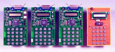
The SLC1657 was tested for code compatibility on two levels. At the logic design level, specific VHDL test benches were created to verify the operation of every op-code. This testing was then double-checked by comparing the operation of finished parts. For example, Figure 1 shows how the SLC1657 was tested against the Microchip PIC16C57. There, three very similar SLC1657 evaluation boards were created using Agere, Altera and Xilinx FPGA parts. These were routed and compared to another board that contains a PIC16C57 made by Microchip Technology. Sample test software routines were then compared on all four boards. The test software included assembly language and compiled 'C' code. Assemblers and compilers from two vendors were used.
It should be noted that there are subtle differences between the SLC1657 and other designs on the market. For the most part, these are the result of the efficient clocking scheme used by the SLC1657, which executes one non-branch instruction on every clock cycle. For a complete list of known incompatibilities, please refer to the SLC1657 Technical Reference Manual.
The SLC1657 Technical Reference Manual, and SLC1657 Datasheet can be downloaded from the following links (they are also included with the SLC1657 source code distribution below):
The SLC1657 source code (including the Technical Reference
Manual) can be downloaded as a 'zip' file here:
Copyright (C) 2003 Silicore Corporation. Verbatim copying and distribution of this FAQ page in any medium is permitted, provided that this notice is preserved. All other rights reserved.
Altera® is a registered trademark of Altera Corporation.
ORCA® is a registered trademark of Agere Systems.
PIC® is a registered trademark of Microchip Technology Inc.
SILICORE® is a registered trademark of Silicore Corporation.
Xilinx® is a registered trademark of Xilinx, Inc.
This page last updated: 30 Sep 2003
6310 Butterworth Lane, Corcoran, MN USA 55340
TEL: 763.478.3567 - FAX: 763.478.3568
www.silicore.net
Home - Sales - Technical Support - Webmaster