

The VHDL component declaration for the Free-6502 core looks like this:
  component core_6502
    port (clk	 	:in std_logic;
          reset	 	:in std_logic;
          irq		:in std_logic;
          nmi		:in std_logic;
          addr	 	:out std_logic_vector (15 downto 0);
          din	 	:in  std_logic_vector (7 downto 0);
          dout	 	:out std_logic_vector (7 downto 0);
          dout_oe  	:out std_logic;
          wr		:out std_logic;
          rd		:out std_logic;
          sync	 	:out std_logic
         );
  end component;
Signal Descriptions
| Signal | Direction | Description |
| clk | Input | The main system clock. All synchronous signals are clocked off the rising edge of clk. |
| reset | Input | An active high reset signal, asynchronous to clk. |
| irq | Input | An active high, level triggered, asynchronous, interrupt input. |
| nmi | Input | A rising edge triggered non-maskable interrupt input. |
| addr | Output | The address bus output. |
| din | Input | Data bus input |
| dout | Output | Data bus output |
| dout_oe | Output | Data bus output enable, used to control external tri-state buffers. Active high. |
| wr | Output | An active high write signal |
| rd | Output | An active high read signal. |
| sync | Output | High during the first byte of an instruction fetch. |
Differences from the original 6502
The most important difference is that the Free-6502 core has a synchronous bus, not asynchronous as the original 6502 had. This is better suited for high-speed ASIC and FPGA implementations.
The data bus is not bi-directional. Instead there are separate input and output "pins" and an output enable. This is to give more flexibility in implementation. If a bi-directional bus is desired, external tri-state buffers can be easily added using the dout_oe signal.
Most/all signals are active high rather than active low. This is a Free-IP Project convention.
Read Cycle
The diagram below shows a basic Free-6502 read cycle:
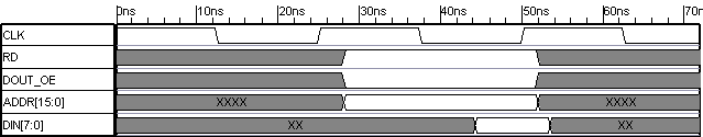
The grayed out areas indicate accesses before or after the read we're interested in.
After the rising edge of the clk the signals rd, dout_oe, and addr become valid. The value of din is latched at the following rising edge of clk.
Write Cycle
This is a basic Free-6502 write cycle:
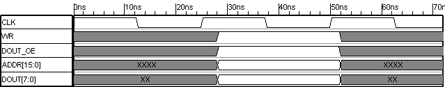
All signals become valid following the rising edge of clk.
It is possible for there to be back to back reads or writes. There can be no idle clock cycles between bus accesses.
Interrupts
The irq input is an active high, level sensitive interrupt. The input is asynchronous with respect to clk, and is synchronized internally.
The nmi input is a rising edge sensitive interrupt. This input is also asynchronous with respect to clk, and is synchronized internally. Due to this synchronization, the minimum pulse width of the nmi input is 4 clock cycles.