XSV Board 1.0 – VHDL
Interfaces and Example Designs

SRAM Interface
Project Supervisor - Peter Sutton
Last Modified: : 14 December 2003
2.0
Files needed for this design
1.0 About this design
The XSV board contains two banks of asynchronous SRAM, each 1 MB in
size. This design presents an interface to these SRAM banks. This interface
provides a simpler method for reading and writing to memory than connecting
directly to the SRAM.
2.0 Files needed for this design
List of Files
·
sram512kleft16bit50mhzreadreq-sv05.vhd
·
sram512kleft16bit50mhzreadreq-sv05c.vhd
·
Outdated files:
§
sram512k32bit50mhz-sv05
§
sram512kleft16bit50mhz-sv01b.vhd
File Descriptions
The SRAM Interface design is not a stand-alone design but rather a
reusable VHDL entity (or module).
The VHDL source files listed above are mutually exclusive – only one is
needed in a given user design. Each file contains a single VHDL module called
“sraminterface”. This module provides a user design with a simple interface for
reading from or writing to SRAM.
Note that the filenames themselves contain information about the content
of the files. The “svXX” suffix on the filenames stands for “source version
XX”. Previous versions of these files are obsolete and have not been released.
sram512kleft16bit50mhzreadreq-sv05.vhd
& sram512kleft16bit50mhzreadreq-sv05c.vhd
The “sraminterface” modules in both these files use the same user-side
interface. The only difference is in their internal timings.
“sram512kleft16bit50mhzreadreq-sv05.vhd” takes 2 clock cycles to perform a read
while “sram512kleft16bit50mhzreadreq-sv05c.vhd” takes only 1 clock cycle to
perform a read. (Both files take 2 clock cycles to perform a write).
Determining which file to use:
In theory, 2 clock cycles should be necessary for a read to be performed
(given the characteristics of the SRAM on the XSV board). Therefore in most
situations “sram512kleft16bit50mhzreadreq-sv05.vhd” should be used. Despite the
theory, the on-chip and on-board timings sometimes eventuate such that one
clock cycle is sufficient for reads to be successfully performed. If this is
the case then “sram512kleft16bit50mhzreadreq-sv05c.vhd” can be used instead.
Outdated
files: sram512k32bit50mhz-sv05.vhd
& sram512kleft16bit50mhz-sv01b.vhd
The “sraminterface” modules in these files have a slightly different
user-side interface from the other two files above. The internal structure of
the modules is also different. They are only listed here because they are used
by some of the other designs in this resource collection. (Note that though these
two files are not the most recent versions, they do still work). The outdated
files are not described in this document (although they are similar to the two
files that are described). For new designs, it is recommended that one of the
other two files above (“sram512kleft16bit50mhzreadreq-sv05.vhd” or
“sram512kleft16bit50mhzreadreq-sv05c.vhd”) be used.
Adding constraints to a UCF
The VHDL modules do not come with their own UCF, but there are constraints
that can be added to the UCF of any design that includes these modules.
Generally these constraints are not essential, but they can improve overall
module timing.
Some helpful constraints to add to a user design that includes an SRAM
interface module are:
·
Constraining the SRAM-side output registers of the
module into IOBs. The following are examples of such constraints:
INST
"user_hierarchy/addrReg_reg<*>" IOB = TRUE;
INST
"user_hierarchy/writeDataReg_reg<*>" IOB = TRUE;
INST "user_hierarchy/CEn_reg" IOB =
TRUE;
INST "user_hierarchy/OEn_reg" IOB =
TRUE;
·
Removing the built-in delay in the input path for the
SRAM data lines. The following is an example of such a constraint:
NET "ldata<*>" IOBDELAY = NONE;
·
Setting the SRAM-side output pins to use the fast slew
setting. The following are examples of such constraints:
NET "laddr<*>" FAST;
NET "ldata<*>" FAST;
NET "lcen" FAST;
NET "loen" FAST;
NET "lwen" FAST;
Note: The net and instance names used above are only examples. The
actual net names will depend on the port names of the top-level entity in the
user design. The fragment of the instance names denoted “user_hierarchy” above
will depend on the name given to the SRAM interface module when it is
instantiated as a VHDL component in the user design.
3.0 Module description
This section describes the SRAM interface module in the two files
sram512kleft16bit50mhzreadreq-sv05.vhd &
sram512kleft16bit50mhzreadreq-sv05c.vhd.
The only filename difference between these two files is that one ends in
“sv05” (i.e. source version 5) while the other ends in “sv05c” (i.e. source
version 5c). Both files contain one VHDL module called “sraminterface”. Both
modules present the same interface to a user design. One description, which
applies to both modules, is given below. (This description does not
apply to the “sraminterface” module in the outdated files listed in the
previous section).
SRAM-side ports
|
Port name: |
Direction: |
Description: |
|
SRAMLeftAddr(18:0) |
Output |
Connects to the SRAM address lines. |
|
SRAMLeftData(15:0) |
Bi-directional |
Connects to the SRAM data lines. |
|
CELeftn |
Output |
Connects to the SRAM /CE pin. |
|
OELeftn |
Output |
Connects to the SRAM /OE pin |
|
WELeftn |
Output |
Connects to the SRAM /WE pin. |
Note: A lower case “n” at the end of a signal name is (often) used to
denote that the signal is low-asserted.
The five ports above must be connected to one of the two banks of SRAM
on the XSV board. The port names themselves suggest that the left SRAM bank
should be used. However this is simply a historic feature of the port naming
scheme. The reality is that the SRAM interface module can be connected to either
bank of XSV SRAM.
The “sraminterface” module gives complete access to one bank of SRAM.
The address and data size details are therefore as follows:
|
No. of addressable locations: |
512 * 1024 = 524 288 = 512K |
|
Width of data at each location: |
16 bits (2 bytes) |
|
Total capacity of one SRAM bank: |
512K * 2 = 1024 KB = 1MB |
Main user-side ports
|
Port name: |
Direction: |
Description: |
|
writeAddr(18:0) |
Input |
Specifies the address to which the user design wishes to write. |
|
writeData(15:0) |
Input |
Specifies the data that the user design wishes to write to SRAM. |
|
readAddr(18:0) |
Input |
Specifies the address from which the user design wishes to read. |
|
readData(15:0) |
Output |
Outputs the data that is read from SRAM. |
|
canWrite |
Output |
High when the “sraminterface” can handle another write request. |
|
canRead |
Output |
High when the “sraminterface” can handle another read request. |
|
doWrite |
Input |
The user design sets this high to make a write request. |
|
doRead |
Input |
The user design sets this high to make a read request. |
The SRAM interface module provides the user design with separate address
and data buses for writing and reading.
Using the SRAM interface
How to
write to an SRAM location
·
Place the address to write to on the “writeAddr” bus.
·
Place the data to be written on the “writeData” bus.
·
Wait for the “canWrite” signal to be high. This
indicates that the module can accept what is called a “write request”.
·
To make the write request, set “doWrite” to high.
“doWrite” can be set to high in the same clock cycle that “canWrite” is high.
On the next rising clock edge after “doWrite”
goes high, the module will register the values on “writeAddr” and “writeData”.
After this time the value on “writeAddr” and “writeData” can be changed. On
subsequent clock cycles the write to SRAM will be performed. “canWrite” will be
low during this time.
·
During the final clock cycle in which the write is
being performed, “canWrite” will go high again. This indicates that the
previous write will be complete at the end of the current clock cycle (in which
“canWrite” goes high). It additionally indicates that another write request can
be made.
How to
read from an SRAM location
·
Place the address to be read from on the “readAddr”
bus.
·
Wait for the “canRead” signal to be high. This
indicates that the module can accept what is called a “read request”.
·
To make the read request, set “doRead” to high.
“doRead” can be set to high in the same clock cycle that “canRead” is high.
On the next rising clock edge after “doRead”
goes high, the module will register the value on “readAddr”. After this time
the value on “readAddr” can be changed. On subsequent clock cycles the read
from SRAM will be performed. “canRead” will be low during this time.
·
During the final clock cycle in which the read is
being carried out, “canRead” will go high again. At the end of the clock cycle
in which “canRead” is high again, the user design must register the value of
the “readData” bus. The user design must register this value at this
time, as it is not registered internally by the module and may change on the
next clock cycle.
“canRead” going high additionally indicates
that another read request can be made.
Additional
notes
·
When making a write request, “writeAddr”, “writeData”
and “doWrite” can be set up in any order, provided that “writeAddr” and
“writeData” have the correct values on the first rising clock edge that occurs
after “doWrite” goes high (with “canWrite” also high).
·
When making a read request, “readAddr” and “doRead” can
be set up in any order, provided that “readAddr” has the correct value on the
first rising clock edge that occurs after “doRead” goes high (with “canRead”
also high).
·
As may already be evident, the signals “canWrite” and
“canRead” always have the same value. This could change in future versions,
however, so it is probably wiser to use the correct signal for the operation
being performed.
Actual module timings
To allow the internal timings of the module to change if necessary, it
is best to use the “canWrite” and “canRead” signals to determine when writes
and reads can be performed and when writes and reads have concluded. However,
for the two files listed in the start of this section, the current timings used
are of course fixed. The timing diagrams below show the various signals timings
for a write operation followed (several clock cycles later) by a read
operation. These diagrams are not designed to highlight the procedure for
making a write or read request, by rather what happens when the module receives
(and acts on) either of these requests. (These diagrams were created using the
Logic Simulator programme in Xilinx Foundation).
sram512kleft16bit50mhzreadreq-sv05.vhd
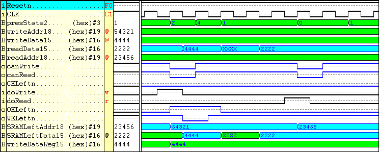
|
Operation: |
No. of clock cycles used: |
|
Write |
2 |
|
Read |
2 |
sram512kleft16bit50mhzreadreq-sv05c.vhd
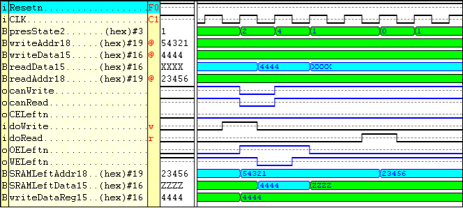
|
Operation: |
No. of clock cycles used: |
|
Write |
2 |
|
Read |
1 |
Note: The version of “sraminterface” in this file performs a read in
only once clock cycle. This means that the “canRead” signal (and “canWrite”
signal) does not actually ever go low when performing a read. However, provided
that the user design follows the protocol given in the “Using the SRAM
interface” section above, the user design will still work correctly with the
SRAM interface module.
4.0 Known problems
These SRAM interface modules have been tested as far as possible. In
particular they work perfectly as part of the PC to SRAM interface design.
There is a known problem that occurs when using the SRAM interfaces as
part of the VGA Controller design. When that design is implemented, small
glitches are often seen in the VGA picture produced. This may be due to a write
or read to SRAM not being performed successfully. We have attempted to track
down and remove this problem, but have been unsuccessful. We cannot be certain
that the source of the problem lies within the SRAM interfaces, but it is
mentioned here nonetheless.