![]()
![]()
While using the X-BLOX library helps optimize some circuits,
others cannot be optimized to use these features. A solution is
to include Xilinx library elements as `components' in VHDL, and
use either already available circuits in the Xilinx libraries, or
to generate one's own circuits with XACT![]() or a schematic entry tool to be included in the design. These
parts can then be optimized to use all features available on a
particular target technology. While this approach requires more
radical VHDL source code modification, the huge gains possible
make this worthwhile for some resources. Isolating these features
in a distinct ENTITY will enhance portability and
restrict code changes to only a few lines of code. (These
resources (RAMs, etc.) will probably also need to be adapted to a
specific ASIC process to yield optimal results.)
or a schematic entry tool to be included in the design. These
parts can then be optimized to use all features available on a
particular target technology. While this approach requires more
radical VHDL source code modification, the huge gains possible
make this worthwhile for some resources. Isolating these features
in a distinct ENTITY will enhance portability and
restrict code changes to only a few lines of code. (These
resources (RAMs, etc.) will probably also need to be adapted to a
specific ASIC process to yield optimal results.)
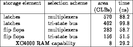
Table 6: Occupied CLBs using five different VHDL
coding strategies for a 16x16 scratch pad RAM. The test circuits
were synthesized using FPGA compiler 3.2a, and routed using
ppr (XACT 5.1). Area results as reported by ppr.
Timing results are pad-to-pad delays as reported by xdelay
and include the propagation delay of input and output pads. Thus,
relative speed differences are more pronounced than they may
appear here.
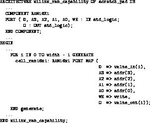
Figure 7: VHDL code for generating a scratch pad
RAM based on the Xilinx XC4000 series RAM capability. Large RAMs
can be assembled using the basic RAM capability available as
macros ( RAM16x1, RAM32x1) in the XACT
library.
Table 6 shows how a design can be optimized by using Xilinx XC4000 features. We compare 5 different designs for a 16x16 RAM. Depending on the VHDL description, Synopsys FPGA compiler generates either flip-flops or latches as storage elements, and uses either a MUX-based signal selection scheme or tri-state buses. These implementation specifics are orthogonal, giving four possible implementations. The synthesis results for these four different architectures show how coding style in VHDL can affect resource consumption, in the example of our 16x16 scratch pad RAM yielding a 4-fold improvement.
A fifth, alternative design is based on the usage of the Xilinx XC4000 capability, where each FG function generator can be reprogrammed to act as 16x1 RAM cell. By using this customization of the RAM cell, the final design uses only 1.4% of the original design.
To generate this design, we use macros from the Xilinx XACT library, which are instantiated as VHDL components in the VHDL description (see figure 7). An alternative way to create RAMs based on the Xilinx RAM capability is to use the memgen tool [Xil94b] from the XACT distribution and include the resulting RAM as COMPONENT.
![]()