![]() tools
tools
.
![]() tools
tools
VHDL : methods and tools
Contents: compiling, simulators, simulator interface, fault simulation, synthesis, high level synthesis, RTL synthesis, formal verification, graphic interfaces, constraint driven evaluation
![]() Analysis,
compilation and elaboration
Analysis,
compilation and elaboration
The simulation process of VHDL entities requires two preliminary steps:
The source code analysis involves the lexicographical and the syntaxical analysis. If both the lexis and the syntax are correct the compiler generates an intermediary code stored in the design library.
There are several kinds of design libraries:
The next step is elaboration which performs several actions such as:
The simulation process starts with several initializing actions such as:
The following figure shows different elements and actions required before the simulation process can start.

Simulation is the essential process required for any design. It is the process which permits to verify the functional characteristics of models at any level of detail and/or abstraction; from system level down to gate level. Simulators use timing characteristics defined before synthesis. After the synthesis the simulation is run using the temporal parameters extracted from the layout. Such a simulation allows dynamic timing analysis. Static timing analysis may also be done by synthesis tools during optimization by simply extracting the delays from the cells used to generate the circuit.
However static analysis is difficult to apply for:
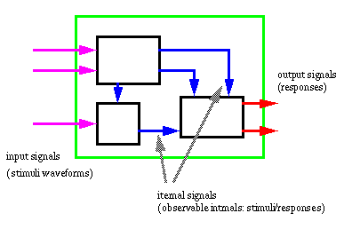
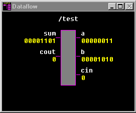
The main role of simulation is the model animation. This allows modeler to observe each unit (entity) response according to the applied stimuli. Given that the models may be built from many interconnected units, the simulation offers the means to observe and o analyze the internal activities visible at the interconnection level.
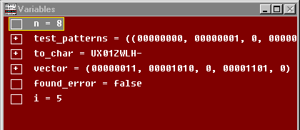
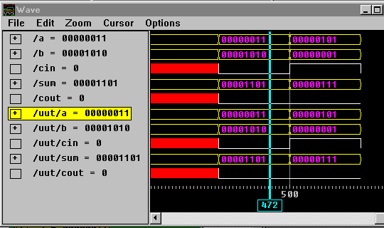
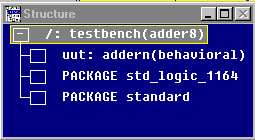
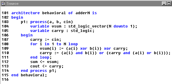
A typical VHDL simulator handles several kinds of windows used to display the simulation results. The following figures show some working windows of Modeltech simulator:


Fault simulation is the simulation of the model with a particular set of input stimuli vectors.
Fault simulation allows to:
The efficiency of functional testing is called fault coverage and is measured by:
fault_coverage (in %) = faults_detected*100/faults_considered
Typical value of fault coverage may be situated between 75% and 99.9%; some faults are always possible !
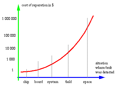
The cost of "repairing" of a functional error is changing rapidly depending on the stage and place of the error detection.
Synthesis is a process of transforming the functional models into the detailed structural models.
There are two levels of digital circuits synthesis:
![]() High
level synthesis proceeds in several steps:
High
level synthesis proceeds in several steps:
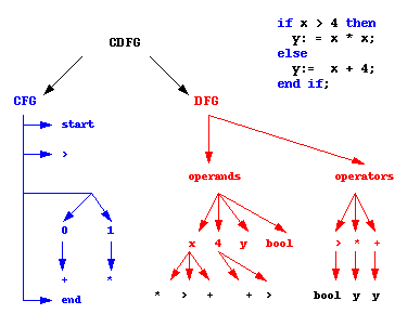
The CDFG is made of two graphs: the DFG for the data dependencies and the CFG for the control. A synthetizable VHDL code is made of concurrent processes. Normall, one CFG is created by process. A global DFG is added to allow the differenet processes to share the ressources.
The CDFGs contain all the control and data dependencies of a givel behavioral model. Scheduling algorithms partition the CDFG into subgraphs where each subgraph is executed in one control step. Each control step corresponds to one state of the controlling finite state machine. Within a control step, a separate functional unit is required to execute each operation assigned to that step. Scheduling a sequencing graph determines the concurrency of the resulting design, and therefore it affects its performance. By the same way, the maximum number of concurrent operations of a given type during the schedule is a lower bound on the number of required hardware resources. In this way the choice of a schedule affects the area (silicon surface) of the implementation.
There are several algorithms used for scheduling:
Their efficiency depends on the application type and on the additional scheduling constraints, for example, related to the resource availability.
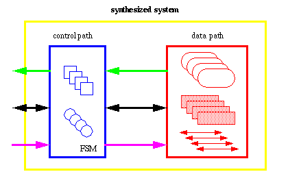
Allocation is used to allocate different kinds of resources to the scheduled execution phases. Normally, it is performed into three steps:
Allocation algorithms generate data-path structure built from interconnected functional units and registers.
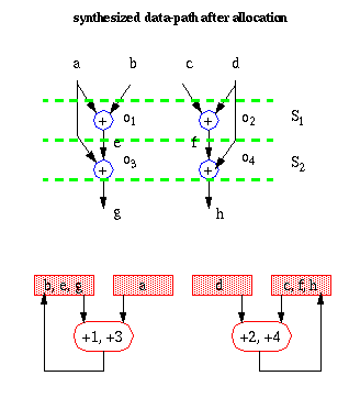
The above example shows how two functional units are allocated to perform four addition operations in two scheduled steps: S1 and S2.
The final phase of high level synthesis is RTL code generation. This code describes the synthesized circuit in terms of architectural elements characteristic for the RTL level.
![]() Register
Transfer Level synthesis
Register
Transfer Level synthesis
RTL synthesis transforms the RTL level descriptions into the corresponding and optimized gate level models.
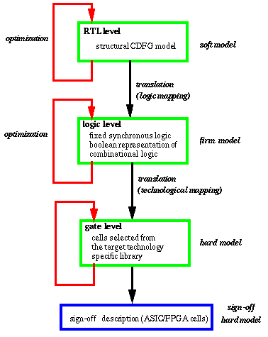
This process includes translation and optimization.
The logic level model is a structural description built from logic gates corresponding to logic operators seen as components
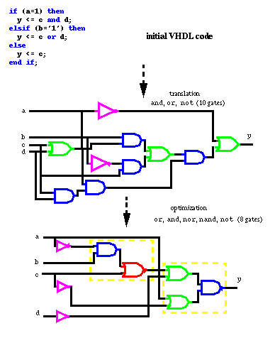
The optimization phase accurs at all intermediate levels (RTL, logic, gate). The constraints provided by the modeler are used to guide the optimization process. The initially generated logic gate net-list undergoes optimization process according to two kinds of constraints:
The default optimization target is minimum circuit size. This optimization involves the use of hierarchical blocks optimized starting from the lower level blocks in a bottom-up process.
![]() Logic optimization
Logic optimization
Once synthesis has translated a design to logic level, all elements seen at RTL level are fixed and only combinational logic is optimized. Optimization at this level performs boolean optimization based on different techniques such as:
The synthesis algorithms operate on multiple level (levels of logic equations) and multiple output basis. They are much more complex and efficient than the traditional methods based on a two dimensional Karnaugh maps.
Example of a two-output function of four arguments: x=f(a,b,c,d); y=f(a,b,c,d)
s = a*b*c
x = s + a*b*d
y = a*b + c + d
after factorization => (6 basic gates)
t = a*b
s = t*c
x = s + t*d
y = t + c + d
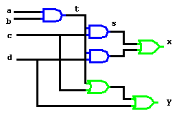
after flattening =>
x = a*b*c + a*b*d
y = a*b + c + d
and after factorization => (4 basic gates)
t = a*b
r = c + d
x = t*r
y = t + r
![]() Gate level optimization
Gate level optimization
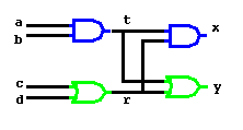
Gate level optimization is related to the gate to transistor mapping. In this process basic logic gates are mapped onto ASIC or FPGA cells. These cells are built from interconnected transistors in this way that negated operations such as nand or nor need less transistors than direct operators such as and or or. The following example illustrates both the logic level and the gate level optimization. Note that simple gates are replaced by a smaller number of gates including nand and nor. Morover, these functionally more complex cells require less transistors to be realized.
Calculate the number of transistors necessary for each scheme?
![]() High
level graphic interfaces and design systems
High
level graphic interfaces and design systems

Speed Electronic was founded in 1987 in Switzerland as an engineering
service company.
It developed simulation models for Nixdorf Computer and has since that
time created major high level models for ESA (European Space Agency) and
other large electronic companies and systems houses in the field of ASIC's,
automotive and micro computer models.
Beside their modeling work, the engineers at Speed developed advanced EDA
software tools to make the generation of HDL models more productive and
provide executable specifications to their customers for design review
and easy design reuse.
In 1992 the company started as a side business to sell its EDA tool speedCHART
for Verilog and VHDL modeling. Today the EDA software and its support is
the main business of the company. There are already more than 1,500 engineers
worldwide, using Speed's tools for the design of complex ASIC's and FPGA's.
Because it grew out of a high skilled group of hard and software engineers,
speedCHART is a very powerful tool, which helps chip designers to increase
their productivity substantially and produce designs which can be reused
easy.
Renoir - Renoir system provides a modern graphical entry to generate VHDL/Verilog synthesizable code from easy to use schematics including well-known forms like:
The modelers can generate powerfull and efficient synthesizable code in just a couple of hours
Mentor Graphics Renoir is a next generation HDL graphical entry tool that can generate Verilog and VHDL from Moore/ Mealy state, flow chart, truth table and block diagrams for FPGA, ASIC and IC. It is available on UNIX (SUN/ HP) and Windows NT/95 platforms. It includes interfaces to logic synthesis, digital simulation, HW-SW co-verification, requirements tools. VHDL and Verilog Intellectual Property (I.P.) is also supported.

Exemplar Logic Inc., a supplier of logic synthesis software for Windows and UNIX platforms, today announced that it is introducing a new synthesis design environment named Leonardo. Leonardo adds support for preservation and manipulation of hierarchical designs and interactive synthesis.
For the first time, Exemplar's users can interactively control synthesis, selectively optimizing different parts of their designs for speed or area. Users can change the design hierarchy, depending on their design needs. Leonardo facilitates "what-if" analysis, allowing users to try alternate scenarios without leaving the Leonardo design environment.
Robert Barker, Exemplar's vice-president of marketing, noted "Over the next few years, FPGA vendors will introduce devices with finer grain architectures, which push the 100K gate limits. These FPGAs require an ASIC-like design methodology that allows designers to design interactively with more control over their synthesis environment. Our roadmap follows this same path."
Exemplar Logic, the number one supplier of programmable logic synthesis software, and Xilinx, the world's largest supplier of programmable logic solutions, today announced that Exemplar's Leonardo synthesis solution is fully certified for the Xilinx XC4000EX family, with unique support for the XC4000EX family's SelectRAM Memory feature. There is a diagram showing the Xilinx flow with Leonardo.
![]()
The Future of FPGAs
A white paper by the company that invented them
Introduction
As programmable logic suppliers accelerate their use of advanced deep submicron
technologies, digital designers can expect to see higher densities and
faster devices at lower voltages that will be more competitive than ever
with traditional ASICs. Within the next decade, Xilinx believes that programmable
logic will become one of the largest segments of the logic market, surpassing
both standard logic and masked gate arrays. This phenomenon will change
how logic is designed, making programmable logic pervasive in many engineering
organizations. This white paper examines a number of fundamental questions
about the changes taking place with high density programmable logic technology.
And it examines how Xilinx, as the inventor of FPGAs and the industry's
leading innovator, is providing answers to those questions.
FPGAs: The New Process Drivers
New field programmable gate arrays (FPGAs) manufactured using advanced
0.35 and 0.25 micron technology and offering in excess of 100,000 logic
gates will be widely available during 1997. In a shift that brings them
to the forefront of progress in semiconductor manufacturing, FPGAs today
are becoming ideal vehicles for driving CMOS process technology development.
It is easier to quickly identify manufacturing process defects in FPGAs,
which are standard SRAM-based devices, than it is in, say, microprocessors.
In addition, ever higher transistor counts in FPGAs and their use of multiple
metal interconnect layers truly stress a CMOS process. For example, the
new Xilinx XC4085XL FPGA, the industry's highest density device scheduled
for delivery during the first half of 1997, is fabricated on a 0.35 micron,
three-layer metal process. The XC4085XL has 16 million transistors, more
than three times the number in Intel's Pentium ProTM
processor. As Xilinx makes the transition to 0.25 micron, five-layer metal
technology in the near future, the company plans to manufacture parts with
more than 30 million transistors. Before the turn of the century, Xilinx
will be using 0.18 micron technology to build devices with 60 million transistors.
Using FPGAs as process drivers ensures that design engineers will have
access to the largest and fastest devices that can be built using any technology.
 Xilinx
SmartSearch provides the best Programmable Logic searching available anywhere.
We're currently indexing over 50 different sites rich with programmable
logic content. You can also constrain your search to focus on any one or
more of the indexed sites. For the Xilinx site you can constrain your search
to look only for general items such as application notes or datasheets,
or search for topic areas such as PCI or DSP.
Xilinx
SmartSearch provides the best Programmable Logic searching available anywhere.
We're currently indexing over 50 different sites rich with programmable
logic content. You can also constrain your search to focus on any one or
more of the indexed sites. For the Xilinx site you can constrain your search
to look only for general items such as application notes or datasheets,
or search for topic areas such as PCI or DSP.
 Once
you have located the information you were looking for, you can stay up-to-date
on any new additions by using SmartSearch Agents! Once you have created
a SmartSearch Agent, you will automatically be notified via email of any
new documents added to any of the 50+ sites we index that match your search
string. You don't have to be a Xilinx customer to take use SmartSearch
Agents. If you haven't already registered for Agents, click
here and we'll get you signed up!
Once
you have located the information you were looking for, you can stay up-to-date
on any new additions by using SmartSearch Agents! Once you have created
a SmartSearch Agent, you will automatically be notified via email of any
new documents added to any of the 50+ sites we index that match your search
string. You don't have to be a Xilinx customer to take use SmartSearch
Agents. If you haven't already registered for Agents, click
here and we'll get you signed up!
![]() HDLs generators
HDLs generators
![]() Schematic generators
Schematic generators