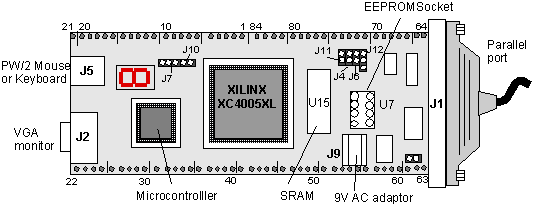
Figure 1: Schematic diagram of the XS40 board.
(XC4005XL FPGA)
The XS40 is a convenient board for implementing and experimenting with FPGA designs. In contrast to the FPGA Demoboard, the XS40 board contains additional components such as a 8031 microcontroller, SRAM (32 KB for the XS-005XL and 128 KB for the XS-005XL+ boards), a 100 MHz programmable oscillator, a parallel port, PS/2 port for a mouse or keyboard, and a VGA monitor port. This makes it a convenient system to implement not only FPGA designs but also microcontroller applications with the FPGA as a coprocessor and the SRAM for data/program storage. The board can be programmed through a parallel port. The FPGA can also be tested using the XSPORT utility that allows you to apply test signals through the parallel port.
The board has a XC4005XL FPGA which contains 9,000 gates and operates at 3.3V but is it 5V tolerant. It has a breadboard interface that allows you to plug the board into a breadboard so that you can easily access its pins. A schematic diagram of the board is given in Figure 1 below. The board can be configured for different purposes, such as use in a design environment (default) or use as a stand-alone board, reprogramming the clock, etc. The mode of operation is determined by jumpers. The settings of the jumpers and the correspondent configurations are explained later on in Table 6
.
Figure 1: Schematic diagram of the XS40 board.
Notice that the FPGA chip is volatile which implies that it needs to be reprogrammed every time you switch off the power supply and restart the board. If you like to use the board by itself without having to reprogram it through the parallel port, you can download the configuration file in an on-board EEPROM. The XS40 board allows you to do so. Every time that you start the board, the configuration file will now be loaded into the FPGA from the serial EEPROM. How to program the EEPROM using the XS40 board is explained in the section on "configuring a FPGA with the XS40 board".
The XS40 board is powered through a 9V DC supply. This can be easily done using a 9V AC adapter (300 mA) which plugs into a 9V DC jack, with a center positive terminal. The board has two voltage regulators that generate the 3.3V for the FPGA and 5V for the rest of the components. Pin 2 of the board is connected to 5V, pin 54 to 3.3V and pin 52 is connected to the ground. See also pins of the FPGA.
The XS40 board contains one 7-segment LED display whose elements are connected to one of the pins of the FPGA. The pin I/O connections of the display to the FPGA are shown in the table below. A 220W resistor is placed between the LED element and the ground to limit the current needed from the FPGA output. A schematic diagram of the LED circuit used in the display and the numbering of the elements is shown in Figure 3. The LEDs are active-high, which implies that they will light up when a logic "1" is applied to their terminal.
Table 1: Pin connection of the 7-segment LED display
|
|
XC4005XL Pin | |
|
|
|
|
|
|
|
|
|
|
|
|
|
|
|
|
|
|
|
|
|
|
|
|
|
|
|
|
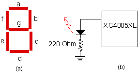
Figure 3: Seven-segment display: (a) LED segments and (b) LED connection
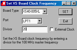
A 100 MHz programmable oscillator is available. The clock is connected to the clock input (GCK1) of the XC4005XL FPGA on pin number 13.
The default setting of the clock on the XS40 V1.4 is 50 MHz. This frequency can be re-programmed by dividing the 100 MHz master clock by any integer from 1 to 2052, resulting in frequencies ranging between 100 MHz and 48.7 KHz.
Programming the clock oscillator
Before reprogramming the oscillator you need to put the oscillator in the programming mode. This is done by placing a shunt on jumper J12 (see Figure 1). Do the following steps (exactly in this sequence):
C:\> XSSETCLK Board_Type Divisor
As an example, in case you want to run the oscillator at 5 MHz (divisor of 20), you would give the following command,
C:\ > XSSETCLK XS40-005XL 20
The XS40 board is programmed through a PC parallel port, using a female DB25 connector on the XS40, labeled J1 in Figure 1. The PC can then transmit signals to the XS40 board for programming the FPGA or testing later on. Communication from the board to the PC is also possible through the status input pins of the PC parallel port.
In case you want to download test signals to the FPGA, this can be done through pins 2 to 9 of the parallel port J1.
Table 2 gives the pin numbers of the J1 connector, the corresponding XC4005 pins and the XSPORT arguments. It should be noted that pins 2 and 3 of J1 are connected to an inverting Schmitt-trigger in order to clean up high frequency clock signals through built-in hysteris. This makes the two pins suitable for clock input signals in sequential circuits. If you are using the XSPORT program, you do not need to worry about the inversion since the program accounts for the inversion of these two signals.
Table 2: Pin correspondence between the parallel port J1, the XS4005 chip and the XSPORT arguments
|
|
|
|
|
( with inverting Schmitt-trigger) |
|
|
|
( with inverting Schmitt-trigger) |
|
|
|
|
|
|
|
|
|
|
|
|
|
|
|
|
|
|
|
|
|
|
|
|
|
|
Note: The pins 32 and 34 correspond to the special purpose pins M0 and M2 of the FPGA which determine the mode of the device at power-up. This implies that in order to use these pins for a regular input signal, you need to place special symbol PADs on the schematic: MD0 and MD2. This will automatically assign the pin numbers 32 and 34 to these pads, respectively.
The XS40 boards are equipped with static RAM that can be used to store
data for FPGA based designs or can be used in conjunction with the microcontroller
to store programs or data. The XS40-005 has 32 Kbyte while the XS4005XL+
has 128 Kbyte of SRAM. The RAM is organized as a 32K x 8 bit, or 128K x
8 bit memory devices. Connections between the memory and the FPGA and microcontroller
are made on the board. A schematic of the memory package and pin names
is shown in Figure 5. The 32Kbyte and 128Kbye memory has 14 and 16 address
pins, respectively. The correspondence between the SRAM pins, the XC4005XL
and the microcontroller pins are given in Table 4. The Chip Enable (/CE1,
/CE2), Output Enable (/OE) and Write Enable (/WE) are active low signals.
The /CE2 pin is always connected to the Vdd while, the /CE1 pin is pulled
high through a 4.7kW resistor in order to disable
the RAM when the FPGA is being configured. This pin is connected to pin
65 of the FPGA and can be driven low when needed. The /OE1 is driven by
the FPGA through pin 61. The /WE signal comes from the microcontroller
(Port 3, pin P3.6) and is also connected to pin 62 of the FPGA.
Figure 5: SRAM memory chip used on the XS40
board (32Kbyte or 128Kbyte)
Table 4: Correspondence between the SRAM, XC4005XL and the microcontroller pins.
|
|
|
|
|
|
|
|
|
|
|
|
|
|
|
|
|
|
|
|
|
|
|
|
|
|
|
|
|
|
|
|
|
|
|
|
|
|
|
|
|
|
|
|
|
|
|
|
|
|
|
|
|
|
|
|
|
|
|
|
|
|
|
|
|
|
|
|
|
|
|
|
|
|
|
|
|
|
|
|
|
|
|
|
|
|
|
|
|
|
|
|
|
|
|
|
|
|
|
|
|
|
|
|
|
|
|
|
|
|
|
|
|
|
|
|
|
|
|
|
* Only for the XS40+ board with the 128KB SRAM
A 8031 microcontroller is resident on-board and is powered by the XS40 power supply. Connections to the FPGA and SRAM are made on the board. The INTEL 8031 is a 8-bit controller with, data and program memory, bi-directional and individually addressable I/O lines and full duplex serial port.
The microcontroller multiplexes the eight lower address bits [A0:A7] and the data bits [D0:D7] on port P0 which is connected to both the SRAM data bus and FPGA. Data between the microcontroller and the SRAM is exchanged through this connection. When the lower address bits are present on this port, the microcontroller will generate an ALE signal that latches the address bits in the FPGA which sends them to the lower eight address lines of the SRAM. For the connections between the FPGA, microcontroller and SRAM see Table 4 and Table 5.
|
|
|
|
|
|
|
|
|
|
|
|
|
|
|
|
|
|
|
|
|
|
|
|
|
|
|
|
|
|
|
|
|
|
|
|
|
|
|
|
|
|
|
|
|
|
|
|
|
|
|
|
|
|
|
|
|
|
|
|
|
|
|
|
|
|
|
|
|
|
|
|
|
|
|
|
|
|
|
|
|
|
|
|
|
|
|
|
|
PC-S4 |
|
|
|
|
|
|
|
|
|
|
|
|
|
|
|
|
|
|
|
|
|
|
|
|
|
|
|
|
|
|
|
|
|
|
|
|
|
|
|
|
|
|
|
|
|
|
|
|
|
|
|
|
|
|
|
|
|
|||
|
|
|
PC-S6 (Status) |
|
|
|
|||
|
|
|||
|
|
|
|
|
|
|
|||
|
|
|
|
|
|
|
|
For the 32KB SRAM, the upper 7 memory address bits, [A8:A14] are connected to the Port 2 of the microcontroller, [P2.0:P2:6]. For the board that is populated with an 128 KB SRAM, the memory bits [A8:A15] are connected to Port 2, [P2.0:P2.7], while memory address bit A16 is connected to pin 16 of the FPGA. Port 2 is also connected to the FPGA so that it can decode the address. For a more complete description of the microcontroller connection, consult the XS40 user manual [1].* Only on the SC40+ board with 128KB SRAM
PS/2 Mouse or Keyboard connector J5
The XS40 board has a connector (J5 in Figure 1) that accepts inputs from a keyboard or a mouse. You will need a keyboard driver circuit that can be downloaded from the XESS homepage, (http://www.xess.com). The Data and Clock lines are connected to port P3.1 and P3.4 of the microcontroller, and to pins 69 and 68 of the FPGA, respectively (see Table 7).
A 15-pin connector (J2) is available to connect a VGA monitor. This can be used to display images on the monitor. In order to do so, you will first need to download a VGA driver circuit to the XS40 board. Examples of drivers are available on the XESS Corp. homepage, (http://www.xess.com). Connections of the VGA port to the FPGA are given in Table 7.
Table 7: Connection of the PS/2 port and the VGA monitor inputs
| VGA Inputs |
|
Microcontroller pin |
| Vertical SYNC |
|
Port P1.7 |
| Horizontal SYNC |
|
|
| Red1 |
|
|
| Red0 |
|
|
| Green1 |
|
|
| Green0 |
|
|
| Blue1 |
|
|
| Blue0 |
|
|
| PS/2 Port | ||
| Data |
|
Port P3.1 |
| Clock |
|
Port P3.4 |
If you are using the board in a normal design environment for downloading a configuration file from a PC through the parallel port, you can leave the default jumper settings. For any other use, select the jumpers settings as explained in Table 6. See Fig. 1 for the jumper numbers.
|
|
|
Description |
|
|
|
Install a shunt for downloading through the PC parallel port. |
|
|
Remove the shunt to configure the XS40 Board from the on-board serial EEPROM (U7). | |
|
|
|
Install a shunt for programming the on-board serial EEPROM (U7). |
|
|
Remove the shunt for normal board use (downloading the configuration file to the FPGA through the parallel port). | |
|
|
|
Install a shunt on pins 1 and 2 (ext) if the 8031 microcontroller program is stored in the external SRAM (U8) of the XS40 Board. |
|
|
Install a shunt on pins 2 and 3 (int) if the program is stored internally in the microcontroller. | |
|
|
(default) |
When the XS40 Board uses the 3.3V XC4000XL type of FPGAs. |
|
|
When the XS40 Board uses the 5V XC400E type of FPGAs. | |
|
|
|
To configure the XS40 Board from the on-board serial EEPROM (U7). |
|
|
Remove the shunt for downloading through the PC parallel port. | |
|
|
|
Install a shunt for downloading through the PC parallel port. |
|
|
To configure the XS40 Board from the on-board serial EEPROM (U7). | |
|
|
|
Place a shunt over pins 1-2 for normal operations when the programmable oscillator is generating a clock signal. |
|
|
Place a shunt over pins 2-3 to set the programmable oscillator frequency. |
Place the jumpers in the default setting, connect the cable between the PC parallel port and the J1 connector, and power up the board. Go to the XSTOOLS/BIN folder and launch the GXSTEST program. This will open the XS Board test utility, shown in Figure 6. Select the proper board type (ex. XS40-005XL) and press the TEST button. A message will appear in the window indicating the status of the test. If the test is successful, the LED on the board will display a 0, otherwise an E will be displayed to indicate an error. If an error occurs, check the parallel port connection and verify that the jumpers are in the proper location.
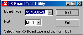
Figure 6: XS Board Test Window (Screen clip from XESS (TM) GXtools)
Created by Jan Van der Spiegel <jan@ee.upenn.edu>;Updated June 4, 2000.