An Introduction to the Concepts of Timing and Delays in Verilog
An Introduction to the Concepts of Timing and Delays in Verilog
The concepts of timing and delays within circuit simulations are very
important because they allow a degree of realism to be incorporated into
the modelling process. In Verilog, without explicit specification of such
constraints, the outputs of pre-defined primitives and user-defined
modules are all assumed to resolve instantaneously (or at least, within
one simulator timestep). This, clearly, is not enough for a designer to
work with, especially since the time taken for changes to propagate
through a module may lead to race conditions in other modules. Some
designs, such as high speed microprocessors, may have very tight timing
requirements that must be met. Failure to meet these constraints may
result in the design failing to work at all, or possibly even producing
invalid outputs. Thus, while the obvious aim of the designer may be to
produce a circuit that functions correctly, it is equally important that
the circuit also conforms to any timing constraints required of it.
This page aims to provide an introduction to these concepts, and in
particular, to the Verilog conventions and techniques for dealing with delays and timing.
Delays can be modelled in a variety of ways, depending on the overall
design approach that has been adopted. These correspond neatly to the
different levels of modelling that have already been introduced, namely
gate-level modelling,
dataflow modelling and
behavioural modelling.
At this level, the delays to be considered are propagation delay through
the gate, and the time taken for the output to actually change state.
These changes of state are grouped into four categories based on the
transition occurring. Each category of change of state has an associated
delay, three of which can be specified by the designer, the fourth being
computed from the other three. The three delays which can be specified,
and the transitions for which they are relevant, are detailed below :
Table 1 : Transition Delays
| Rise Delay |
0, x, z -> 1 |
| Fall Delay |
1, x, z -> 0 |
| Turn-Off Delay |
0, 1, x -> z |
0, 1, x and z take their usual meanings
of logic low, logic high, unknown and high impedance. (Reminder
: High impedance means that the net is not directly being driven by
anything and so is floating. Thus it has neither a high nor a low logic
value.) Any or all of these delays can be specified for each gate by use
of the delay token `#'. If only one value is specified, it
is used for all three delays. If two are given, they are used for the
rise- and fall-delays respectively. The turn-off delay (the time taken
for the output to go to a high impedance state) is taken to be the minimum
of these values. Alternatively, all three values can be explicitly set.
The use of delays is illustrated below for the 2-input multiplexor given
in an earlier example.
module multiplexor_2_to_1(out, cnt, a, b);

   /*
    *  A 2-1 1-bit multiplexor
    */

   output out;
   input  cnt, a, b;
   wire	  not_cnt, a0_out, a1_out;

   not # 2    n0(not_cnt, cnt);        /* Rise=2, Fall=2, Turn-Off=2 */
   and #(2,3) a0(a0_out, a, not_cnt);  /* Rise=2, Fall=3, Turn-Off=2 */
   and #(2,3) a1(a1_out, b, cnt);
   or  #(3,2) o0(out, a0_out, a1_out); /* Rise=3, Fall=2, Turn-Off=2 */

endmodule /* multiplexor_2_to_1 */
(Since none of the gates used above are tri-state devices, the value
for the Turn-Off delay should not be specified, and the internally
calculated value for this delay will never be used in such
gates.)
The fourth category of transitions is for a change of state to an unknown
value (i.e. 0, 1, z -> x), and its
delay value is taken to be the minimum of the above three.
As dataflow modelling does not use the concept of gates, but instead has
the concept of signals or values, the approach taken to allow modelling of
delays is slightly different. The delays are instead associated with the
net (e.g. a wire) along which the value is transmitted. Since values can
be assigned to a net in a number of ways, there are
corresponding methods of specifying the appropriate delays.
- Net Declaration Delay
- The delay to be attributed to a net can be associated when the
net is declared. Thereafter any changes of the signals being
assigned to the net will only be propagated after the specified
delay.
e.g.
wire #10 out; assign out = in1 & in2;
If either of the values of in1 or in2
should happen to change before the assigment to out has
taken place, then the assignment will not be carried out, as input
pulses shorter than the specified delay are filtered out. This is
known as inertial delay.
- Regular Assignment Delay
- This is used to introduce a delay onto a net that has already
been declared.
e.g.
wire out; assign #10 out = in1 & in2;
This has a similar effect to the code above, computing the value of
in1 & in2 at the time that the assign
statement is executed, and then storing that value for the specified
delay (in this case 10 time units), before assigning it to the net
out.
- Implicit Continuous Assigment
- Since a net can be implicitly assigned a value at its
declaration, it is possible to introduce a delay then, before that
assignment takes place.
e.g.
wire #10 out = in1 & in2;
It should be easy to see that this is effectively a combination of
the above two types of delay, rolled into one.
At this level of abstraction, the circuit is modelled by assigning values
to variables, some of which correspond to the the inputs and outputs of
the module in question. Again, there are number of different types of
delay associated with this style of programming :
- Regular Delay Control
- This is the most common delay used - sometimes also referred to
as inter-assignment delay control.
e.g.
#10 q = x + y;
It simply waits for the appropriate number of timesteps before
executing the command.
- Intra-Assignment Delay Control
- With this kind of delay, the value of
x + y is
stored at the time that the assignment is executed, but this value
is not assigned to q until after the delay period,
regardless of whether or not x or y have
changed during that time.
e.g. q = #10 x + y;
This is similar to the delays used in dataflow modelling.
Examples using delays
Given the earlier information on delays, it is now time to look at some
designs that incorporate delays, and examine the effect that they have on
their outputs.
The design below is for a full-adder,
written using gate-level modelling techniques. (Note :
The generate and
propagate signals, G and
P from the diagram, are not given as outputs here.
However, some designs which attempt to improve on the overall data rate
may make use of them, thus requiring them to be added to the list of
module outputs - see the carry skip adder
later on.) The code given specifies some of the delays described
above - the first of the two graphs shows the output of an identical
circuit but without any delays, while the second
shows the actual output from the code below. [View full source code :
Delays / No delays]
module full_adder(sum_out, carry_out, a, b, carry_in);

   /*
    * A gate-level model of a 1-bit full-adder
    */

   output carry_out, sum_out;
   input  carry_in, a, b;
   wire	  one_high, generate, propagate;

   xor #(3,2) x0(one_high, a, b);
   xor #(3,2) x1(sum_out, one_high, carry_in);
   and #(2,4) a0(generate, a, b);
   and #(2,4) a1(propagate, one_high, carry_in);
   or  #(3)   o0(carry_out, generate, propagate);

endmodule /* full_adder */
|
Note :
|
The clk signal in the graphs below is not required for
the operation of the circuit, and is provided purely to illustrate
the delay in the output signals.
|
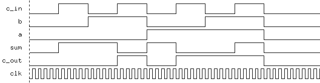 Full Adder : Output - no delays
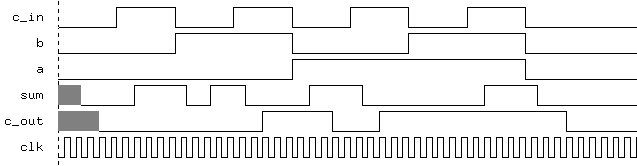 Full Adder : Output - delays as specified
As can be seen from the output graphs, the effect of the delays on the
timing of the outputs can be quite significant, possibly even resulting in
the correct output for the sum not being available until after the inputs
have changed again. This could lead to race conditions or worse, so the
rate at which the inputs are allowed to change must be controlled.
(See the section on setup and
hold times.) Since this is usually governed by a clock, the
clock period chosen must be longer than the maximum delay time between the
inputs changing and the outputs settling - but this may differ depending
on the actual inputs. For example, with the rise and fall delays for all
of the gates given as above in the code for the full_adder, the output of
logic high on the
Full Adder : Output - delays as specified
As can be seen from the output graphs, the effect of the delays on the
timing of the outputs can be quite significant, possibly even resulting in
the correct output for the sum not being available until after the inputs
have changed again. This could lead to race conditions or worse, so the
rate at which the inputs are allowed to change must be controlled.
(See the section on setup and
hold times.) Since this is usually governed by a clock, the
clock period chosen must be longer than the maximum delay time between the
inputs changing and the outputs settling - but this may differ depending
on the actual inputs. For example, with the rise and fall delays for all
of the gates given as above in the code for the full_adder, the output of
logic high on the carry_out line will take between 5 and 8
time units to appear, if the module had previously been outputting a logic
low. However, the transition to a logic low from a logic high, for the
same output, will take between 7 and 9 time units.
|
Exercise 1 :
|
Calculate the best and worst delays for both rising and falling
transitions on the sum output.
|
Answers
|
The timing constraints imposed upon each full adder must allow for the
worst case of each of these transitions, so the inputs must stay constant
for at least a period of 9 time units.
When these adders are combined, as in the 4-bit ripple carry adder below, the delays become cumulative,
since the maximum delay for each carry_out to ripple
(propagate) to the next unit must be allowed for in the overall
design.
|
Exercise 2 :
|
What delay is required before ALL of the outputs of a 4-bit
ripple carry adder can be guaranteed to have settled?
|
Answers
|
The code below uses the full_adder module defined earlier.
The graphs show sample sections of the output signals, which illustrate
the differences between a circuit using full_adders with no delays, and
one using full_adders with delays as specified earlier. [View full source
code : Delays / No delays]
module ripple_carry_4_bit(sum_out, carry_out, a, b, carry_in);

   /*
    *  A gate-level model of a 4-bit ripple carry adder
    */

   output [3:0]	sum_out;
   output	carry_out;
   input [3:0]	a, b;
   input	carry_in;
   wire [2:0]	ripple;

   full_adder f_a0(sum_out[0], ripple[0], a[0], b[0], carry_in);
   full_adder f_a1(sum_out[1], ripple[1], a[1], b[1], ripple[0]);
   full_adder f_a2(sum_out[2], ripple[2], a[2], b[2], ripple[1]);
   full_adder f_a3(sum_out[3], carry_out, a[3], b[3], ripple[2]);

endmodule /* ripple_carry_4_bit */
|
Note :
|
The clk signal in the graphs below is not required for the
operation of the circuit, and is provided purely to illustrate the delay
in the output signals.
|
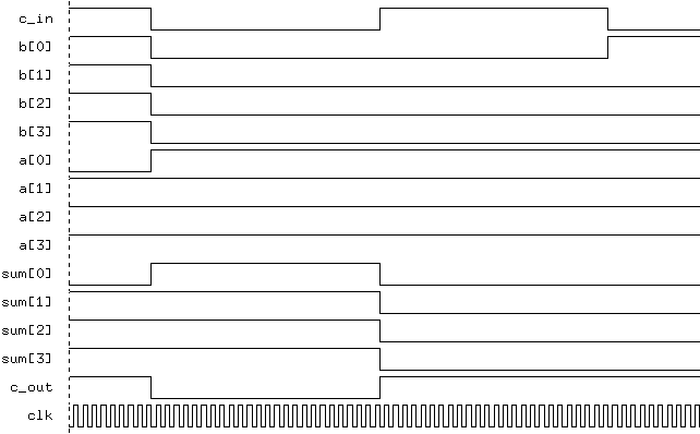 4-bit Ripple Carry Adder : Output - no delays
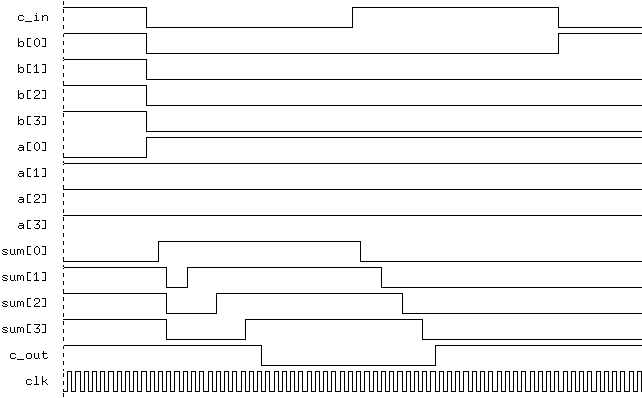 4-bit Ripple Carry Adder : Output - delays as specified
The delay required could be determined from the output graphs, if the
worst case input vectors were used. The worst case input vectors are the
ones that generate the longest overall delay though the design. For many
complex designs, there may be no easy way of determining these vectors,
but for the adder used in this example, it can be seen that the worst case
vectors will be the ones that cause each
4-bit Ripple Carry Adder : Output - delays as specified
The delay required could be determined from the output graphs, if the
worst case input vectors were used. The worst case input vectors are the
ones that generate the longest overall delay though the design. For many
complex designs, there may be no easy way of determining these vectors,
but for the adder used in this example, it can be seen that the worst case
vectors will be the ones that cause each full_adder module to
propagate a carry from one stage to the next, as
this has the longest critical path through the module.
|
Exercise 3 :
|
Work out the worst case input vectors
(i.e. a, b and
carry_in) for the 4-bit ripple carry
adder.
|
Answers
|
Knowing the worst case vectors allows tests to be run to confirm the
minimum period for which the inputs must be stationary. This is important
as it determines the maximum data rate through that part of the circuit -
often a crucial consideration in many modern designs. Such an analysis
may result in an alternative solution, with a higher data rate, being
required.
The carry skip adder offers a
significant speed improvement over the ripple carry adder, if the
propagate signals from the individual full-adders are
available. Combining these (using and gates) allows a
propagate signal for the block to be generated. This extra
signal means that in some cases, blocks will not need to wait for an
earlier carry to ripple all the way through each of the earlier blocks.
Rather, if it can be determined that a particular block (e.g. bits 4
to 7) will propagate any carry into that block, and the
carry_in is already known, then that carry can skip
around the block, and be passed into the next block (i.e. bits 8 to
11). This gives a considerable saving in time as the carry signal
need now only pass through two gates - the AND and the
OR - rather than the eight it would otherwise have to
negotiate in the ripple_carry_4_bit module. For this to
work, however, it is necessary to be able to set the carry_in
of each of the blocks to LOW each time any of the inputs
a or b are changed.
|
Exercise 4 :
|
What happens if this is not done?(Hint : Look at what happens
when a block does not generate a carry.)
|
Answers
|
|
Exercise 5 :
|
How could this be overcome?(Hint : Consider changing the
combinational logic between blocks.)
|
Answers
|
There are many other improved adder designs that are even faster than
this, but they are beyond the scope of these examples.
As has just been seen, the two main types of delay used in behavioural
model code, are regular delays and intra-assigment delays. Although the
differences in their actions may not be immediately obvious, they are
perhaps best illustrated by the use of blocking and
non-blocking assignments. Regular delays are most often used
with blocking assignments, and intra-assignment delays are most often used
with non-blocking assignments.
- Blocking Assignments
- Blocking assignments are the most basic of the assignment
operations, and simply copy the value of the expression at the right
hand side of the
= operator to the variable on the left
hand side. However, if two assignments that depend on each other are
scheduled at the same time, e.g. an attempt to swap two variables,
such as :
always @(posedge clk) a = b;
always @(posedge clk) b = a;
then a race condition occurs, and both a and
b will end up with one of the values. The value that
they are both left with will depend on which of the assignments was
scheduled first.
- Non-blocking Assignments
- Non-blocking assignments eliminate the possibility of race
conditions in situations like this, as at the time that the assignment
operation is executed the expression on the right hand side of the
<= operator is copied to an internal temporary variable,
which is then copied to the variable on the left hand side. All of
the `reads' for a particular timestep are carried out before any of
the `writes', and so values can be safely swapped as below :
always @(posedge clk) a <= b;
always @(posedge clk) b <= a;
This time, the code has the intended effect.
Without any explicit delays, all assignments take place in the same
simulator time step, but this does not mean
that they all execute simultaneously. The order of their execution is
still important.
Below are four separate modules. Each uses a different combination of
assignment type and delay type.
|
Exercise 6 :
|
Look at the code below and, for each of the different modules,
write out the time and the values of all of the registers, each
time any of them changes value.
|
Answers
|
|
Note :
|
In the following examples, the event queuing system is assumed to be
stack-based, with later events being pushed onto the end of the
stack, but read from the front. However, the implementation of the
queuing system is not specified in the Verilog language
specification, so this need not necessarily be the case. Hence,
the order in which events scheduled for the same time step in
separate blocks will occur is non-deterministic (i.e. cannot be
predicted) and will depend on the particular implementation of the
queuing system for the specific version of Verilog that you are
running.(On our system, the stack-based system appears to be
used.)
|
module blocking;

   reg[7:0] a, b, c, d, e;


   initial begin
      $monitor($time, " :\ta = %d\t", a,
	       "b = %d\tc = %d\t", b, c,
	       "d = %d\te = %d", d, e);
      #50 $finish;
   end

   initial begin
         a = 2;
         b = 5;
      #1 a = c;
      #1 a = d;
      #2 a = 4;
      #2 a = 7;
         b = 6;
      #2 a = d;
      $display("a, b - done");
   end

   initial begin
         c = 1;
         d = c;
         e = a;
      #2 e = d;
         c = 0;
         d = 3;
      #5 c = a;
         d = 1;
         d = 2;
      $display("c, d, e - done");
   end

endmodule /* blocking */
|
module non_blocking;

   reg[7:0] a, b, c, d, e;


   initial begin
      $monitor($time, " :\ta = %d\t", a,
	       "b = %d\tc = %d\t", b, c,
	       "d = %d\te = %d", d, e);
      #50 $finish;
   end

   initial begin
         a <= 2;
         b <= 5;
      #1 a <= c;
      #1 a <= d;
      #2 a <= 4;
      #2 a <= 7;
         b <= 6;
      #2 a <= d;
      $display("a, b - done");
   end

   initial begin
         c <= 1;
         d <= c;
         e <= a;
      #2 e <= d;
         c <= 0;
         d <= 3;
      #5 c <= a;
         d <= 1;
         d <= 2;
      $display("c, d, e - done");
   end

endmodule /* non_blocking */
|
module blocking_intra;

   reg[7:0] a, b, c, d, e;


   initial begin
      $monitor($time, " :\ta = %d\t", a,
	       "b = %d\tc = %d\t", b, c,
	       "d = %d\te = %d", d, e);
      #50 $finish;
   end

   initial begin
      a = 2;
      b = 5;
      a = #1 c;
      a = #1 d;
      a = #2 4;
      a = #2 7;
      b = 6;
      a = #2 d;
      $display("a, b - done");
   end

   initial begin
      c = 1;
      d = c;
      e = a;
      e = #2 d;
      c = 0;
      d = 3;
      c = #5 a;
      d = 1;
      d = 2;
      $display("c, d, e - done");
   end

endmodule /* blocking_intra */
|
module non_blocking_intra;

   reg[7:0] a, b, c, d, e;


   initial begin
      $monitor($time, " :\ta = %d\t", a,
	       "b = %d\tc = %d\t", b, c,
	       "d = %d\te = %d", d, e);
      #50 $finish;
   end

   initial begin
      a <= 2;
      b <= 5;
      a <= #1 c;
      a <= #1 d;
      a <= #2 4;
      a <= #2 7;
      b <= 6;
      a <= #2 d;
      $display("a, b - done");
   end

   initial begin
      c <= 1;
      d <= c;
      e <= a;
      e <= #2 d;
      c <= 0;
      d <= 3;
      c <= #5 a;
      d <= 1;
      d <= 2;
      $display("c, d, e - done");
   end

endmodule /* non_blocking_intra */
|
When modelling circuit delays, there are a number of options available to
the modeller in terms of how to deal with attributing the delays
around the circuit model. The three most commonly used techniques are
distributed delay, lumped delay and pin-to-pin
delay.
- Distributed Delay
- The distributed delay method requires delays to be assigned to every
element of the circuit - then the delay between any two points can be
calculated by adding together the delays of the components through
which the signal being monitored passes.
- Lumped Delay
- This is similar to the distributed delay approach, except that it is
only modules (rather than their component parts) that are assigned
delays. Normally, the delay assigned to the module is the longest
path through it, to ensure that the model reflects the worst case
performance.
- Pin-to-pin Delay
- (This technique is sometimes also referred to as the path
delay method.) Delays are specified for each input to output
pin pairing, rather than being associated with specific elements.
This can be advantageous as it means that details of the internals of
the module need not be known for the analysis to be carried out.
The behavioural modelling techniques mentioned earlier allow for the
distributed delay and the lumped delay methods to be implemented without
any further special commands. However, in order to use the pin-to-pin
method, some way to specify the timings to use is required.
Verilog provides a set of commands for just this purpose. These
timing-related commands can only be used within a block delimited by the
keywords specify and endspecify, which appears
within a module definition in the same way that behavioural modelling code
does in an initial begin...end or an
always...begin..end block. The specify blocks
allow the timing for single- or multi-bit path delays to be configured,
and also provide a convenient notation for simplifying any changes that
may need to be made to a particular timing delay.
specify
  (a => out) = 9;
  (b => out) = 7;
endspecify
|
Parallel Connections
The => notation can only be used when the source and
destination ports, a and out
respectively in this case, are of the same (bit-)width. Hence
a and out could both be single- or
multi-bit vectors. (e.g. reg a, out;
or reg [3:0] a, out;)
|
specify
  (a *> out) = 9;
endspecify
|
Full Connections
The *> notation may be used when every bit of the
source port is to be associated with every bit of the destination
port. The two ports need not be the same width.
(e.g. reg [3:0] a; reg [7:0] out;)
|
specify
  specparam a_to_out = 9;

  (a => out) = a_to_out;
endspecify
|
"specparam"
Statements
specparam statements are local definitions
(i.e. local to this specify...endspecify
block) that may simplify the task of changing values for
a large set of delays. The use of these statements for all timing
specifications is recommended. Should any of the delay values
assigned to a set of connections change, it is now only necessary
to change the value in the specparam statement,
rather than all of the parallel or full connections.
|
specify
  specparam a_high = 2;
  specparam a_low  = 4;

  if  (a) (a => out) = a_high;
  if (~a) (a => out) = a_low;
endspecify
|
Conditional Path Delays
Conditional path delays (or state dependent path delays)
can be used to set up different delays through a module according
to the state of one or more control signals. The keyword
if is the only one that can be used - unusually,
there is no corresponding else. The
control clause can be any normal expression.
|
Pin-to-pin timings can also be expressed in terms of rise-, fall- and
turn-off times. (See the earlier section on gate
level modelling.) Different delays can be specified for each
possible signal transition, but only in certain combinations, and the
order in which they are to be declared must be strictly observed. The
allowable combinations limit the number of values that may be specified in
any one statement to be 1, 2, 3, 6 or 12 only. The
permitted combinations are as follows :
Table 2 : Pin-to-pin Transition Timings
| Number of parameters |
Used for... |
| 1 |
All transitions.
|
| 2 |
|
Rise and Fall times.
|
|
Rise :
|
0 -> 1, 0 -> z,
z -> 1
|
|
Fall :
|
1 -> 0, 1 -> z,
z -> 0
|
|
| 3 |
|
Rise, Fall and Turn-Off times.
|
|
Rise :
|
0 -> 1, 0 -> z
|
|
Fall :
|
1 -> 0, 1 -> z
|
|
Turn-Off :
|
z -> 0, z -> 1
|
|
| 6 |
The following transitions in this order :
0 -> 1, 1 -> 0,
0 -> z, z -> 1,
1 -> z, z -> 0
|
| 12 |
The following transitions in this order :
0 -> 1, 1 -> 0,
0 -> z, z -> 1,
1 -> z, z -> 0,
0 -> x, x -> 1,
1 -> x, x -> 0,
x -> z, z -> x
|
If the x transitions are not specified, a pessimistic
approach is taken to ensure worst case timings. Any transition from an
unknown (x) to a known (0,
1 or z) state will take the maximum of
the specified times, while a transition from a known state to an unknown
state will take the minimum of the specified times. (e.g. if 6 values
have been specified, a 0 -> x transition will
take the minimum of the delays specified for a 0 ->
1 or a 0 -> z transition.)
All of the examples that seen so far have been of combinatorial logic.
However, timing is equally important in sequential logic, if not more so.
Sequential elements, such as flip-flops, have set timing constraints that
must be observed if they are to work correctly. Two of these, the
setup and hold times specify the amount of time for
which the data input must not change before and after the rising clock
edge, respectively. Failure to observe these constraints may result in
unexpected behaviour from the element.
To facilitate checking for violations of these (and other) timing
constraints, Verilog has a number of system tasks (identified by the
`$' prefix). The two relevant calls here are
$setup and $hold.
	      $setup(data_line, clk_line,
	      limit);
|
data_line is the name of the signal which is to be
monitored for constraint violations, clk_line is the
event (name and transition of the signal) with reference to which
the timing constraints are measured, and limit is the
period before the event on the
clk_line (normally a rising edge) during which the
data_line signal is not allowed to change. If the
signal breaks this constraint, an error is generated.
|
	      $hold(clk_line, data_line,
	      limit);
|
$hold is very similar to the $setup
system task, except that its first two arguments are in the
opposite order, and that the period it specifies is
after an event on the clk_line.
|
These (and the other timing-related functions) can only be called from
within specify blocks. Such functions are not restricted to
use with sequential circuits - they may be used on any circuit where
events can be seen to occur with respect to some other event. Use of the
$setup and $hold tasks is probably best
illustrated by the examples after the next section.
Up until now, all of the timing and delay values have been measured in
terms of simulator timesteps, with no reference to real time.
Verilog allows different timescales (mappings from simulator
timesteps to real time) to be assigned to each module. The
`timescale directive is used for this :
`timescale reference_time_units /
      time_precision
where reference_time_units and time_precision are
values with a measurement - the two values need not use the same
measurement (e.g. `timescale 10 us / 100 ns
), but can only be specified to the nearest 1, 10 or 100
units. The reference_time_units is the value attributed to the
delay (#) operator, and the time_precision is the
accuracy to which reported times are rounded during simulations.
`timescale directives can be given before each module to
setup the timings for that module, and remain in force until overridden by
the next such directive.
The example chosen to illustrate the use of the $setup and
$hold system tasks is an implementation of an iterative
solution to the Towers of Hanoi problem, details of which can be
found elsewhere.
This solution also incorporates a Start button,
which can be pressed and held down for as long as desired. Upon release
of the button, the circuit will output the sequence of moves required to
solve the the puzzle for the set number of disks (in this case, 5).
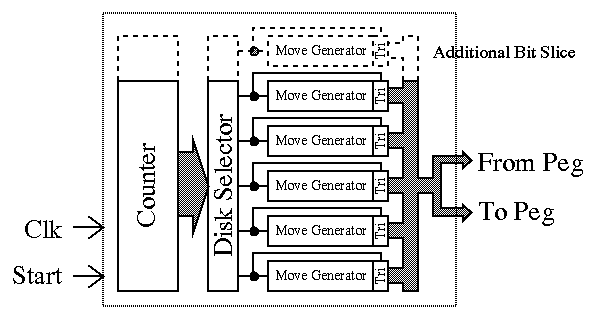
The basic design of the system is illustrated below.
 The code for this is also presented here :
/****************************************************************************\
 *                                                                          *
 *                            The Towers of Hanoi                           *
 *                                                                          *
\****************************************************************************/

/*
 *  Setup up some global parameters, for ease of change.
 */

`define clk_period 20
`define setup_time 4
`define hold_time  1


/****************************************************************************\
 *                                                                          *
 *               'Basic building block' module definitions                  *
 *                                                                          *
\****************************************************************************/

module toggle(q, qbar, clk, toggle, reset);

   /*
    *  A mixed style model of a T-type (toggle) flip-flop,
    *  with a reset line and delays on the outputs.
    *  This first part is behavioural code.
    */

   output q, qbar;
   input  clk, toggle, reset;
   reg	  q;

   always @(posedge clk)
      if (reset == 1)
	 #5 q = 0;
      else if (toggle == 1)
	 #6 q = ~q;

   /*  This part is dataflow-style  */

   assign #1 qbar = ~q;

endmodule /* toggle */

module effr(q, clk, enable, reset, d);

   /*
    *  A behavioural model of an E-type (enable) flip-flop
    *  with a reset signal, and delays on the outputs.
    */

   output q;
   input  clk, enable, reset, d;
   reg	  q;

   /*
    *  This next block checks for timing violations of the
    *  flip-flop's setup and hold times.
    */

   specify
      $setup(d, posedge clk, `setup_time);
      $hold(posedge clk, d, `hold_time);
   endspecify

   /*
    *  This is the actual code for the E-type.
    */

   always @(posedge clk)
      if (reset == 1)
	 #5 q = 0;
      else if (enable == 1)
	 #6 q = d;

endmodule /* effr */

module effs(q, clk, enable, set, d);

   /*
    *  Another behavioural model of an E-type, this time with
    *  a set line, and delays on the outputs.  The same timing
    *  checks as before are implemented here, too.
    */

   output q;
   input  clk, enable, set, d;
   reg	  q;

   specify
      $setup(d, posedge clk, `setup_time);
      $hold(posedge clk, d, `hold_time);
   endspecify

   always @(posedge clk)
      if (set == 1)
	 #5 q = 1;
      else if (enable == 1)
	 #6 q = d;

endmodule /* effs */


/****************************************************************************\
 *                                                                          *
 *    Now, the more complex modules for implementing the actual solution    *
 *                                                                          *
\****************************************************************************/

module evenSlice(bus, oneOut, zeroOut, clk, init, oneIn, zeroIn);

   /*
    *  A dataflow model of one bit slice of the full moves generator.
    *  The only differences between this module and the oddSlice one
    *  are in the initialisation values.  (Note the types of the
    *  flip-flops used.)
    */

   inout [3:0] bus;
   output      oneOut, zeroOut;
   input       clk, init, oneIn, zeroIn;

   wire	       enable, tq, tqbar;
   wire [1:0]  toPeg, fromPeg, new;

   toggle tog (tq, tqbar, clk, oneIn, init);
   effr   to0 (toPeg[0], clk, enable, init, new[0]);
   effs   to1 (toPeg[1], clk, enable, init, new[1]);
   effs from0 (fromPeg[0], clk, enable, init, toPeg[0]);
   effr from1 (fromPeg[1], clk, enable, init, toPeg[1]);

   assign #2 oneOut  =  oneIn & tq;
   assign #2 zeroOut = zeroIn & tqbar;
   assign #2 enable  = zeroIn & tq;

   assign #2 new[1] = ~(toPeg[1] & fromPeg[1]);
   assign #2 new[0] = ~(toPeg[0] & fromPeg[0]);

   assign bus = (enable == 1) ? {fromPeg, toPeg} : 4'bz;

endmodule /* evenSlice */

module oddSlice(bus, oneOut, zeroOut, clk, init, oneIn, zeroIn);

   /*
    *  See the comments for the evenSlice module.
    */

   inout [3:0] bus;
   output      oneOut, zeroOut;
   input       clk, init, oneIn, zeroIn;

   wire	       enable, tq, tqbar;
   wire [1:0]  toPeg, fromPeg, new;

   toggle tog (tq, tqbar, clk, oneIn, init);
   effs   to0 (toPeg[0], clk, enable, init, new[0]);
   effs   to1 (toPeg[1], clk, enable, init, new[1]);
   effs from0 (fromPeg[0], clk, enable, init, toPeg[0]);
   effr from1 (fromPeg[1], clk, enable, init, toPeg[1]);

   assign #2 oneOut  =  oneIn & tq;
   assign #2 zeroOut = zeroIn & tqbar;
   assign #2 enable  = zeroIn & tq;

   assign #2 new[1] = ~(toPeg[1] & fromPeg[1]);
   assign #2 new[0] = ~(toPeg[0] & fromPeg[0]);

   assign bus = (enable == 1) ? {fromPeg, toPeg} : 4'bz;

endmodule /* evenSlice */

module start_button(go, clk, press);

   /*
    *  A gate level model of the start button, with the functionality
    *  as described elsewhere.
    */

   output  go;
   input   clk, press;
   wire	   e_out, not_press;
   supply1 vdd;

   /*
    *  This block checks that the pulse with on the input line is
    *  wider than 3, otherwise it is invalid.
    */

   specify
      specparam min_time = 3;
      $width(posedge press, min_time);
   endspecify

   effs       st_0 (e_out, clk, vdd, press, vdd);
   not #(1)    n_0 (not_press, press);
   and #(2,1)  a_0 (go, e_out, not_press);

endmodule /* start_button */

module tower(from_peg, to_peg, done, clk, start);

   /*
    *  This is a dataflow model of the actual move generator - to
    *  be thought of as a stack (or tower) of modules, each of which
    *  with one disk of the puzzle.
    *
    *  It brings together all of the other modules, and presents a
    *  clean interface to the outside world, taking a 'start' signal
    *  and returning a 'done' signal, once the sequence has been
    *  completed.
    */

   output [1:0]	from_peg, to_peg;
   output	done;
   input	clk, start;
   wire [4:0]	oneOut, zeroOut;
   wire [3:0]	bus;
   wire		init;
   supply1	vdd;

   start_button  st_0(init, clk, start);
   oddSlice  rung0 (bus, oneOut[0], zeroOut[0], clk, ~init, vdd, vdd);
   evenSlice rung1 (bus, oneOut[1], zeroOut[1], clk, ~init,
		         oneOut[0], zeroOut[0]);
   oddSlice  rung2 (bus, oneOut[2], zeroOut[2], clk, ~init,
		         oneOut[1], zeroOut[1]);
   evenSlice rung3 (bus, oneOut[3], zeroOut[3], clk, ~init,
		         oneOut[2], zeroOut[2]);
   oddSlice  rung4 (bus, oneOut[4], zeroOut[4], clk, ~init,
		         oneOut[3], zeroOut[3]);

   assign from_peg = bus[3:2];
   assign to_peg   = bus[1:0];
   assign done     = oneOut[4];

endmodule /* tower */


/****************************************************************************\
 *                                                                          *
 *  The final stimulus module is used to check that the tower module works  *
 *  properly                                                                *
 *                                                                          *
\****************************************************************************/

module stimulus;

   /*
    *  This is a behavioural model.  It simply instantiates the tower
    *  module, provides it with inputs and monitors its outputs.
    */

   reg	      clk, button;
   wire [1:0] from, to;
   wire	      done;

   tower t_0(from, to, done, clk, button);

   initial begin
      clk = 0;
      forever #(`clk_period / 2) clk = ~clk;
   end

   initial begin
      button = 0;
      #40 button = 1;
      #50 button = 0;
   end

   always @(posedge clk)
      #(`clk_period - 1) $display($time, "  From peg %d To peg %d",
				  from, to);

   always @(posedge clk)
      if (done == 1) #`clk_period $stop;

endmodule /* stimulus */
The design has been implemented using bit slice techniques to
allow for easy extension to different numbers of bits (which correspond to
the number of disks in the problem). Each new disk to be catered for
requires the counter and the disk selector to be extended, and a new move
generator with its tri-state outputs to be attached to the bus. This is a
very good methodology to adopt when designing circuits that may be
extended. In this case, another point to be borne in mind is that the
move generators require to be initialised to different values depending
on whether the number of disks is even or odd.
The code makes use of many of the delay
techniques covered earlier, as well as the setup and hold checks.
|
Exercise 7 :
|
Copy the above code to a file, and run it though the Verilog
compiler. Now change the clock period to half of its current value,
and run the code again. What happens?
|
Answers
|
Setup and hold violations allow the maximum rate at which data can be
clocked through the sequential elements of a circuit to be determined.
However, there may be other constraints on the circuit which affect the
overall data rate.
|
Exercise 8 :
|
Change the clock period to 15, and re-run the code. What
happens this time? Why does this occur?
|
Answers
|
|
Exercise 9 :
|
Determine the maximum clock frequency with
which the circuit will function correctly.
|
Answers
|
This example should have given a good idea of the sort of techniques
employed in modelling circuits, making use of delays and timing checks.
Obviously, it has not covered all of the concepts presented earlier, but
has shown a typical use of many of them.
As a final note, the issue of clocking on both positive and negative edges
should be addressed. While this may seem to be an attractive option, for
example clocking data signals on the rising edge and control signals on
the falling edge, it normally does not have the intended effect
of doubling the maximum clock frequency of the circuit in question.
Consequently, while there may not be any directly adverse effects of using
both positive and negative edges of a clock, common synchronous design
practices tend to shy away from this, preferring to keep the design
'clean' by using only one edge of the clock signal to latch all
values.
Last modified: Mon Oct 27 11:43:15 GMT 1997
by Gerard M. Blair