Digital Logic and Microprocessor Design with VHDL ?Enoch Hwang
 |
Projects & Circuits |
Digital Logic and Microprocessor Design with VHDL
Get your own copy from
Amazon.com .
.
The following is a list of interesting projects that you can easily implement.
DE2-70:
Documentations
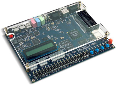
DE2:
Documentations,
LCD Basic,
I2C
UP2:
Documentations,
10-bit Up Counter,
VGA Controller,
HiLo Game,
EC-1 processor,
EC-2 processor,
EC-3 processor,
MIPS processor
UP3:
Documentations,
Nios Development Board:
Documentations,
Web server
Nios II Soft-core uProcessor:
Documentations,
Basic Nios II,
Audio Nios II
Projects using Quartus II v7.2 and implemented on the DE2 development board.
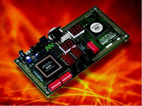
Projects using Quartus II v7.2 or Max+Plus II and implemented on the UP2 development board.
-
Documentations for the UP2
UP2 User Manual v3
Article on how to build hardware from software
-
Counter
A schematic implementation of the 10-bit up-counter with parallel load.
-
VGA Controller
A basic VGA controller for the UP2 development board.
VHDL implementation using Max+Plus II
VHDL implementation using Quartus II
Schematic implementation using Quartus II
The article on building this VGA controller is found
here.
Equipment requirements: Quartus II or Max+Plus II, UP2 board.
-
Hi-Lo Number Guessing Game
A dedicated microprocessor (FSM control unit) for playing the Hi-Lo number guessing game.
Equipment requirements: Max+Plus II, UP2 board.
-
The EC-1 general-purpose microprocessor as discussed in Chapter 12 of my book.
VHDL implementation
Verilog implementation
Schematic implementation
-
The EC-2 general-purpose microprocessor as discussed in Chapter 12 of my book.
VHDL implementation
Verilog implementation
Schematic implementation
-
The EC-3 general-purpose microprocessor. This is a complete FSMD and FSM+D implementations using VHDL of a fairly extensive instruction set
including instructions for subroutines, stack, and interrupts.
Documentation
VHDL FSMD implementation
VHDL FSM+D implementation
-
The MIPS processor
from the book Computer Organization and Design, 3rd Edition, by Patterson and Hennessy.
This is an implementation of the multicycle MIPS processor based on the datapath of Figure 5.28 on page 323 and the control unit of Figure 5.37 on page 338.
The instructions implemented are: ADD, ADDI, SUB, AND, OR, SLT,
LW, SW, BEQ, JUMP, OUTPUT, and HALT. The last two instructions are not from the MIPS processor.
The sample program will count down from 10 down to 0.
Equipment requirements: Quartus II, UP2 board.
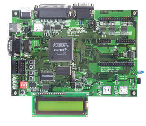
Projects using Quartus II v7.2 and implemented on the UP3 development board.

Projects implemented on the Nios Development Kit Stratix Edition board.