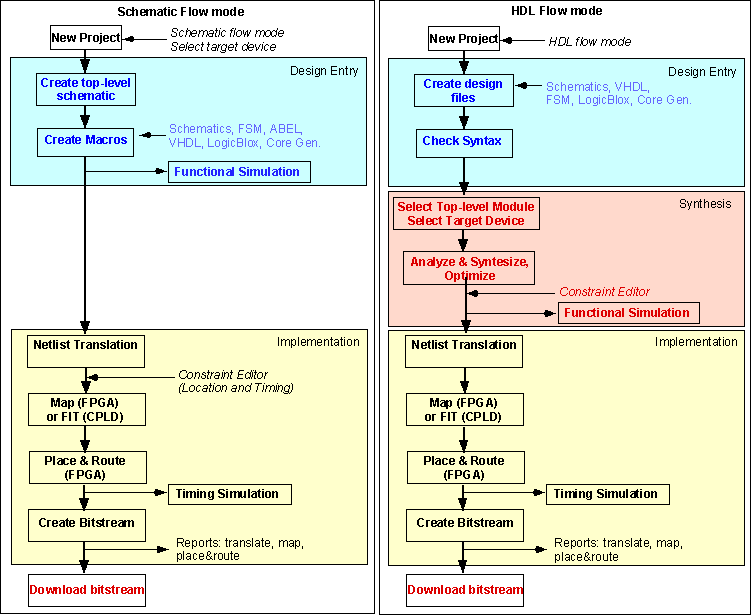
Figure 1: Design and Implementation sequence of a Schematic (a) and
HDL flow (b) projet.
Figure 1: Design and Implementation sequence of a Schematic (a) and
HDL flow (b) projet.
In this section we will briefly discuss how to create macros in the Schematic Flow mode. You will learn how to create a macro from a schematic, an ABEL and VHDL file, and how to instantiate these macros in a top level schematic. The procedure for creating macros in the HDL Flow mode is very similar. The main difference is the synthesis step as illustrated in Figure 1 above.
We will illustrate the creation of macros using a simiple example of
a 4-bit comparator that compares two 4-bit words and outputs a logic "1"
if the two words are identical, otherwise a logic "0". However, to keep
the comparator more general, the X inputs can be selected from two different
words (A or B) using a 2:1 multiplexer. If the X (i.e. A or B) and Y signals
are the same, the comparator generates a logic "1", otherwise a logic "0". Figure
2 shows the overall schematic. Each comparator compares one bit of each
word. If the four comparators outputs Zi are equal to "1", the AND gate
will give a "1".
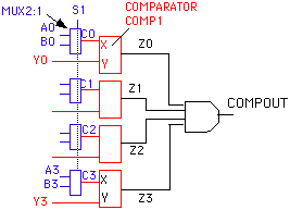
Figure 2: Two 4-bit word comparator
We will build this circuit in a modular way, using macros. First, we will create a macro for a 1-bit comparator using the schematic entry tool. We will call this macro "COMP1ME". Then, we will build a macro for the 2:1 multiplexer using HDL. Once these two macros are created, we will build the overall circuit schematic (top level schematic).
User-defined macros can be created in several ways. A convenient method is using the Symbol Wizard which can be used to create both schematic and HDL based macros. With the Symbol Wizard tool you create the symbol first and the underlying schematic or HDL file later.
An alternative way to create a user-defined macro is to create the underlying source file first, such as the schematic or HDL file. If the source file is a schematic, go to HIERARCHY menu -> CREATE A MACRO SYMBOL from the Current Sheet in the schematic editor. In case of a HDL file, go to PROJECT menu -> CREATE MACRO in the HDL Editor. If the underlying macro is a State Machine Diagram, go to the PROJECT menu -> CREATE MACRO. A symbol will be created and placed in the project library in all three cases. We will illustrate these methods in the next example.
Lets first create a new project, called "COMP4ME" (go to the FILE menu ->CREATE NEW PROJECT in the Project Manager window). Fill out the Project Name, Directory, select "Schematic Flow", fill out the Device Family (ex. XC400XL), Part (4005XLPC84) and Speed as you did in the section on "Schematic Entry".
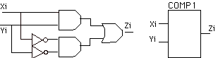
Figure 3: 1-bit comparator schematic and symbol
a1. Using the Symbol Wizard
i. Create a Symbol
Open the Schematic Entry tool by clicking on the Schematic Entry icon in the Project Manager Window.
Lets use the Symbol Wizard tool. In the Schematic Entry window, go to the TOOLS menu -> SYMBOL WIZARD. A Wizard will guide you through by asking several questions.
ii. Creating an underlying schematic file for the macro
On the schematic of the macro you can now draw the logic gates (Figure 3) for the COMP1ME macro. Creating the schematic is basically the same as explained above in section on "Schematic Entry". However, there are two difference:
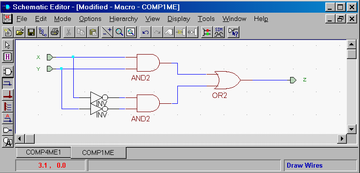
Figure 4: 1-bit comparator schematic used as a macro (Screen clip from
Xilinx Foundation Foundation software).
When finished save the schematic. To check if the macro has been created, in the schematic editor go to FILE->OPEN->MACRO. The macro COMP1ME should appear. At this point you can simulate the macro.
To simulate the macro, go to the TOOLS -> SIMULATE CURRENT MACRO in the Schematic Editor window of the macro COMP1ME. This will open the simulator. You can now add the signals and stimuli. You can do a functional simulation and verify the operation of the 1-bit comparator.
Alternatively, you can first place the macro on the main schematic. You will find the macro in the Symbol Toolbox of the Schematic Editor under the name COMP1ME. Next, go to the simulator by clicking on the SIM icon on the top toolbar.
In case you created a schematic as part of another project and would like to use this schematic as a macro in a new project you can do so.
An alternative way to create the macro, is to create the schematic first and then the symbol. In that case you will open a new sheet and draw the schematic. For the input and output ports you need to use I/O terminals and not IPAD, OPAD, IBUF and OBUF as explained above. When finished with the schematic of the macro, you need to create a symbol. This is done in the same way as above. Go to the HIERARCHY ->CREATE MACRO SYMBOL FROM CURRENT SHEET menu. The Create Symbol window will appear. For the Symbol Name, type in the name you want to give to the 1-bit comparator. Lets call it "COMP1ME2". Make sure that all input and output pins appear in the Pin section of the Create Symbol window. In the comment field, type any comment you like. Click OK. The symbol will be added to the SC Symbols toolbox list. You can now use the newly created macro (symbol) as you would do with any other symbol. You can complete your top level schematic at this point, or create another macro.
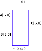
Figure 5: Symbol for the quad 2:1 MUX.
Lets assume that you have already created a project called COMP4ME of which the macro for the MUX will become part.
i. Open the Project: COMP4ME and open the Schematic Editor window.
ii. Create new symbol
In case you want to modify the symbol, such as changing the shape of the symbol, adding, renaming, or removing I/O pins, you can do so. In the Schematic Editor window, select TOOLS -> SYMBOL EDITOR. Or you can also click on the macro symbol on the schematic. The Symbol Properties window will open. Click on Symbol Editor. This will open the HDL Editor window. You can now define the ABEL file in the HDL Editor window as explained next.
iii. Create an ABEL macro
C = !S1 & A # S1 & B;
|
|
|
|
|
|
|
|
|
In order to simplify the expression we made use of sets in the ABEL
description (A = [A3..A0], etc.). Each member of the set will undergo the
same logic
operations (see ABEL Primer - section 5b on Sets). Thus the above expression
is equivalent to four individual expressions:
C0 =!S1 & A0 # S1 & B0;
:
C3 =!S1 & A3 # S1 & B3;Figure 6 shows the ABEL editor window. Notice that the sets for A, B and C are already defined. Enter in the equation section the expression for C.
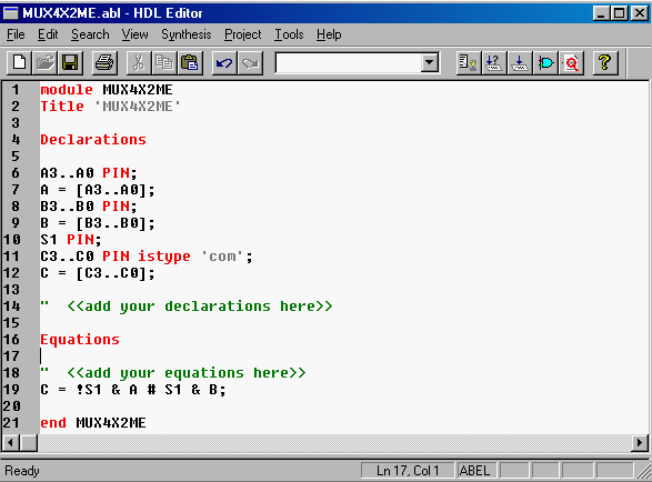
Figure 6: ABEL editor window for the quad 2:1 multiplexer (Screen clip
from Xilinx Foundation (TM) Foundation software).
As was noted above, this method has the annoying feature that it will expand the buses for the signals A[0:3], B[0:3] etc. which makes the schematic quickly unwealdy, particularly when working with wide buses.
i. Open the Project: COMP4ME and open the Schematic Editor window.
ii. Create new symbol
In case you want to modify the symbol, such as changing the shape of the symbol, adding, renaming, or removing I/O pins, you can do so. In the Schematic Editor window, select TOOLS -> SYMBOL EDITOR. Or you can also click on the macro symbol on the schematic. The Symbol Properties window will open. Click on Symbol Editor. This will open the HDL Editor window. You can now define the ABEL file in the HDL Editor window as explained next.
iii. Create a VHDL macro
  C(0)<= ((not S1) and A(0)) or (S1 and B(0));
  C(1)<= ((not S1) and A(1)) or (S1 and B(1));
  C(2)<= ((not S1) and A(2)) or (S1 and B(2));
  C(3)<= ((not S1) and A(3)) or (S1 and B(3));
Figure 7 shows the VHDL Editor window.
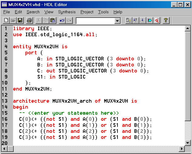
Figure 7: VHDL Editor window for the 2:1 MUX of Figure 8.4. (Screen
clip from Xilinx Foundation (TM) Foundation software).
We are now ready to design our 4-bit comparator of Figure 2 using the macros for the 1-bit comparator and the quad 2:1 MUX. Go to the Schematic Editor window. The sheet COMP4ME.sch will open.
i. Adding macro and logic symbols
Lets add the 1-bit comparator cells by clicking on the Symbol icon on the left toolbar. Type comp to go to the COMP1ME symbol. Select COMP1ME and place it on the schematic. Then click on the symbol to place multiple copies of it. Next add the quad 2:1 MUX. Add next the 4 input AND gate (AND4). If the symbol name of COMP1 does not show and you want to display it, select the symbol and double click. In the Symbol Properties window, press the Attributes key and select "Show Symbol Name".
Lets assume that we want to implement the 4-bit into a FPGA or CPLD.
Thus we need to indicate the input and output pads (unless you want to
make another macro for the 4-bit comparator; in that case follow the same
procedure as above). First you have to add the input buffers. Select IBUF4
in the SC Symbol window and place it on the schematic. Do this for each
input A, B and Y (see Figure 8). For the
S1 input signal, place a single IBUF. Then add the OBUF. Next, place the
input pads (IPAD4) and output pad (OPAD) to indicate the connection to
the actual pin of the FPGA or CPLD.
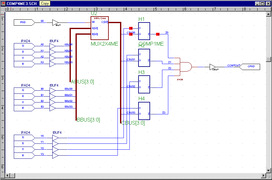
Figure 8: Top level schematic of the 4-bit comparator (Screen clip
from Xilinx Foundation (TM) Foundation software).
ii. Adding wires and net names
Connect the IPADS to the IBUF and the OBUF to the OPAD using the Draw Wire command. Also, connect the output of the AND gate to the input of the OBUF and the output of the four 1-bit comparators to the input of the 4-input NAND gate.
Next, we want to label the input, output nets and the compartor outputs. Select the Add Net Names icon on the left toolbar. The Net Name window will pop up. Enter the Net Name A0. To speed up the net naming, select the REPEAT button. Every time you click on a net, a new name will be placed and the name index will be incremented by one. Press the ESC key to finish the command. Do the same of the B inputs and the Z outputs of the 1-bit comparators. Don't forget to name the S1 input net. Next, we will use the Draw Buses command to connect the inputs.
To connect the IBUF4 outputs to the MUX inputs A[3:0] and B[3:0] we
will use the Draw Bus command. Click on the Draw Buses icon or go to the
MODE -> DRAW BUSES menu. Click on the input A[3:0] of the MUX and draw
the bus as shown in Figure 9. Click to make a corner in the bus. Click
on the right mouse button or double click to end the bus. An Add Terminal/Label
or Edit Bus window will appear, as shown in Figure
9. If not, double click at the end of the bus. In the window enter in the
Name
field: ABUS. Select a bus width: from 3 to 0. This bus is not an input
or output bus, so the I/O marker should say None. Click OK. Do the
same for the B-bus and the C bus and call this bus BBUS and CBUS, respectively.
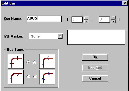
Figure 9: Edit Bus window (Screen clip from Xilinx Foundation (TM)
Foundation software).
Now we can connect the inputs of the 1-bit comparators to the buses. This is done by clicking on the Draw Bus Taps icon or going to the MODE menu ->DRAW BUS TAPS. Click first on the bus name ABUS to select the bus you want to tap into. The status line will show that the first bus tap ABUS0 (usually the member with the lowest index) has been selected for placement. Next click the cursor on the A0 output of the first input buffer (IBUF4) (least significant bit). Then, click on A1 outputs of the 2nd, 3rd and 4th buffer. When finished click on the ESC key twice. Repeat the process for the BBUS and CBUS as shown in Figure 8. Make sure that the tap numbers correspond to the numbers of the input signal (A0 connected to ABUS0, A1 to ABUS1, etc.).
Note: The default start number for the tap is 0. You can use the up and down arrow keys to select which bus bit will be tapped. If the down arrow key was pressed last, the bus tap numbers will decrease.
If you want to connect a single wire to a bus, you need to draw a wire that starts or ends at the bus. Next you will need to label the wire with the name of a bus member to which you want to connect. For instance, you want to access the most significant bit in the carry-cout bus (CBUS). You need to name the wire CBUS3. If you do not name the wire, there will be no connection (a warning will be generated) or if you give it different name from the bus, there will be an error.
To simplify a schematic, you can combine buses and individual wires into a complex bus. This is done by naming the complex bus with a compound label. A compound label consists of several label names (with or without ranges), separated with commas. To enter a compound label, use the following format:
NAME[F:L:I],NAME,NAME[F:L],...where F is the first number, L is the last number, and I is the interval between the numbers in the range. If no interval is specified, the interval is 1. As an example we could combine the LED-OUT buses and the Error signal in a complex bus with the name
LED_ONE[6:0], LED_TWO[6:0],ERRORor we can use a selected number of wires: LED_ONE[3:0], LED_TWO[4:2],ERROR
It is important that each of the bus segments, such as LED_ONE[6:0] have been defined beforehand. For more information about buses, in the Schematic Entry window, select HELP -> SCHEMATIC EDITOR HELP CONTENTS. In the help window select INDEX and type buses.
I/O terminals vs. PADS.
In case you decide to use this schematic as another macro and do not intend to implement this particular schematic in a FPGA or CPLD, you do not need to add PADS and BUFFERS. In that case, when you draw the input buses to connect the inputs A and B, you will indicate in the Add Terminal/Label window (Figure 5) that the bus is an input (or output, if appropriate). The name of the bus will now be the name of the inputs to the macro. To create a macro from the schematic go to the HIERARCHY ->CREATE MACRO SYMBOL FROM CURRENT SHEET menu. When the schematic is finished save it.
iv. Going down the hierarchy
To push into a schematic of a macro, select the "H" icon (Hierarchy icon) and double click on the desired macro symbol (ex. comp1). To go back to the upper level schematic, double click on the background of the lower level schematic.
v. Netlist and Integrity Test
When the schematic is finished you can create a netlist and do an integrity test. This is done by going to the OPTIONS menu-> CREATE NETLIST. When finished, it is always a good idea to check that the schematic has no electrical design rule errors. This is done from the OPTIONS menu -> INTEGRITY TEST. You can now also generate a EDIF netlist by going to the OPTIONS menu -> EXPORT NETLIST.
vi. Simulation
You can now do a functional simulation of the schematic as was explained in the section on "Simulation". The only difference is the presence of buses. In order to assign signals to the individual inputs of the A and B bus, you need to expand the bus into the individual signals. This is done by selecting the bus A or B in the Waveform Viewer window and then going to the SIGNAL->BUS -> FLATTEN. You can now assign outputs of the binary counter to the individual A and B inputs. You can click on the Bus Expansion Icon on the top toolbar to collapse or expand the bus (after creating it first), or go to the SIGNAL -> BUS -> COMBINE menu after selecting the signals you want to collapse into one bus (in this case, it will be A0, A1, A2 and A3). The signals on a collapsed bus are displayed in HEX notation (unless othewise specified).
Other macros:
One can add other types of macros to the top-level schematic such as
a Finite State Machine (FSM) macro, LogiBLOX or CORE Generator module.
The procedure is similar to what was done for an ABEL or VHDL macro. For
instance, to create a FSM macro, open the FSM editor by clicking on the
State Editor in the Project Manager window. Follow the procedure as explained
in the section on the "State
Editor".
Copyright, 1999, Jan Van
der Spiegel <jan@ee.upenn.edu>; created August 26, 1997; Updated
by Jan Van der Spiegel; May 17, 2000.