![]()
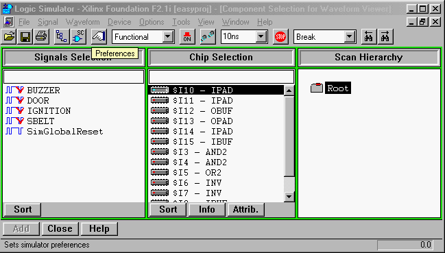
Figure 1: Logic Simulator window (Screen clip from Xilinx (TM) Foundation software)
A functional simulation is done to verify the operation of the
circuit. Click on the "Simulation" icon in the Project Manager window (Figure
4 of the Introduction section) or select TOOLS -> SIMULATION/VERIFICATION
-> GATE SIMULATOR from the Project Manager window. The current version
of the design will be loaded. If a windows appears with the message: "Schematic
Netlist easyproj is older than schematic. Update netlist from Schematic
Editor?" click YES. The Foundation Logic Simulator window will pop up with
a Waveform Viewer window shown in Figure 1.
![]()
Figure 1: Logic Simulator window (Screen clip from Xilinx (TM) Foundation software)
ii. Selecting input and output signals
To simulate the circuit you do the same as if you were testing the circuit in the lab: add input signals to the input pins and view the input and output waveforms. Thus the first step is to specify the input signals. This is done by clicking on the CHIP icon (select component) on top of the Waveform Viewer window or by going to the SIGNAL menu ->ADD SIGNAL. Another window will appear, called the Component selection window, as shown in Figure 2.
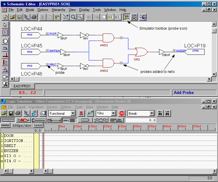
In the Component Selection window, select the inputs you want to add to the waveform viewer and click the "Add" button or double click the signal name. Do this for all inputs and outputs. When done, click on the CLOSE button. The selected signals will appear in the Waveform Viewer window.Figure 2: Component Selection windows (Screen clip from Xilinx (TM) Foundation software)
You can also select test pins by going back to the schematics and add probes to the wires:
Next you need to add a stimulus to the input signals.
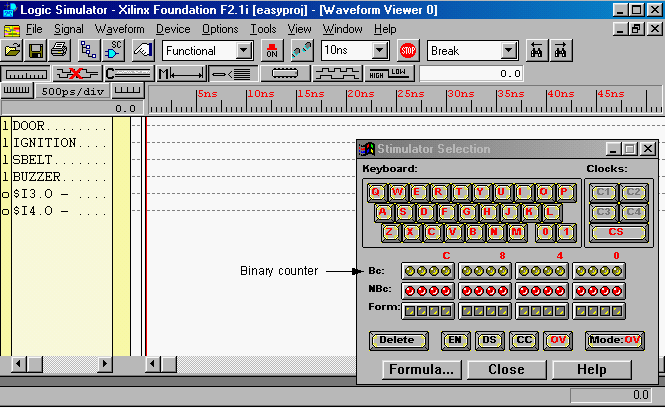
Figure 4: Stimulator window and Simulation window (Screen clip from Xilinx (TM) Foundation software)In our case we need to use only three outputs of the counter. We will use the lower three bits of the Bc counter. Click on the signal name in the Waveform viewer first (Ex. DOOR) so that it is highlighted, then click on the most right side counter output (labeled 0). The name B0 will appear after the signal name in the Waveform Viewer. Do the same for the other three input signals (select the next two counter outputs B1 and B2, respectively).
You can also assign a keyboard key to the signal, to manually toggle the signal. This is done by selecting one of the keys on the Keyboard section in the Stimulator window. For more information, click the HELP button. When done, close the Stimulator Selection window.
iv. Defining the Frequency of the free-running Counter
One can define the clock frequency of the free-running counter. Go to the OPTIONS-> PREFERENCES menu in the Waveform Viewer.Under the Simulation section, click on the B0 period drop-down list and select the required period. The frequency will automatically adjust. The precision depends on the type of simulation. A functional simulation requires less precision (e.g. 1ns) while a timing simulation requires higher precision (e.g. 100ps or less).
v. Doing the simulation and viewing the waveforms
At this point we can do a functional simulation. Choose "Functional" from the pull down menu at the top of the simulator window. Then click on the Simulation step (footstep) icon at the top of the window to initiate the simulation. The inputs and corresponding output waveform are displayed, as shown in Figure 5. To change the size of the step, use the pull down menu next to the step icon. You can also change the scale of the time axis by clicking on the ruler icon on top of the Signal list. The time scale is displayed as well.
You can switch back to the schematics window by clicking on the SC icon
in the Simulator window. The schematic window will show the actual logic
levels (0 or 1) of each of the signals added to the Waveform Viewer window.
The results will be shown on the schematic for the signals you have added
to the Waveform Viewer window. You can add additional signals by clicking
on the Probe icon in the SC Probes window. Click on the nets that you want
to display. Figure 5 shows the results of the
simulation in both the Simulator and Schematic windows. The value of the
logic signals displayed on the schematic corresponds to the last time step
displayed in the Simulator window or to the position of the cursor (17.5ns
in Figure 5). One can view the values of the logic signals on the schematic
as one steps though all the values. This is a convenient way to check the
operation of the circuit.
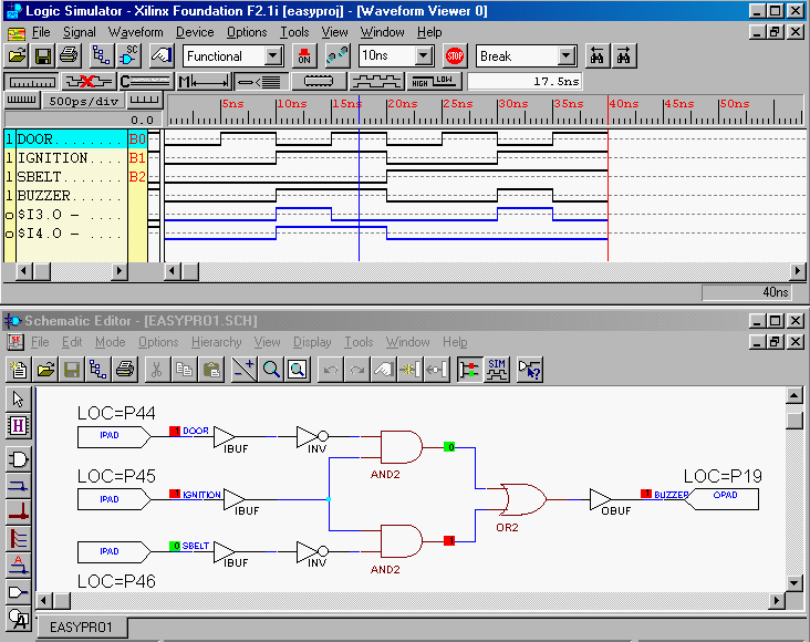
Figure 5: Results of the simulation shown in the Simulator and Schematic windows.(Screen clip from Xilinx (TM) Foundation software)
Now you can verify if the circuit performs as expected. If problems occur, check your logic or the schematic.
To clear the waveform and start the simulation over again, go to the WAVEFORM -> DELETE -> ALL WAVEFORMS WITH POWER ON menu item.
Notice that the functional simulation tells you only about logic but not about timing. This means that no information about gate delays (and thus max. frequency), hazards or set-up and hold-time violations can be extracted from the functional simulation. Once you have compiled your design for a specific device, you can do the timing analysis.
vi. Displaying signals as buses
If you have many signals to display, it may be more convenient to group them into a "Bus". This can be done by first selecting the signals you want to group and then going to the SIGNAL -> BUS -> COMBINE menu. The value of the signals of the bus are displayed in HEX notations (unless otherwise specified). You can also flatten a bus by going to the SIGNAL -> BUS ->FLATTEN menu. An example of a simulation with buses is shown in Figure 6. To see the signals in a bus without flattening it, click on the BUS on/off (expand) icon on the top toolbar in the waveform viewer. The LSB of a bus is denoted by a "*" and the MSB by a "$". All other signals are denoted by a "+" sign. If the bus is backwards (i.e. the LSB becomes the MSB), you can switch the direction by selecting the bus, right clicking and selecting BUS-> Change DIRECTION.
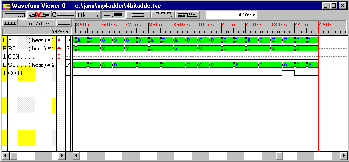
Figure 6: Waveform Viewer window in which the signals have been combined
into buses
(Screen clip from Xilinx (TM) Foundation software)
We mentioned that the 3rd row of LEDs in the Stimulator Selection Window is used to assign user-defined values (or formulas) to a signal. Formulas can be used to assign values to a single signal or a bus. This is done by clicking on the Formula button in the Stimulator Selection window. This will bring up the Set Formulas window, shown in Figure 7.
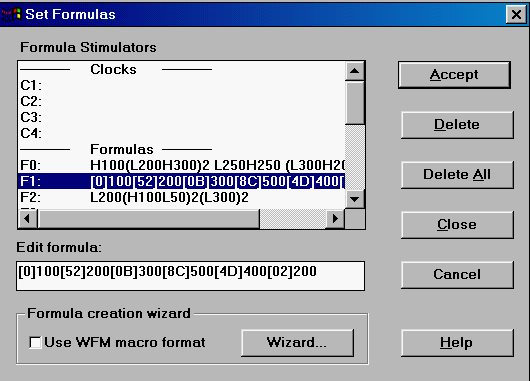
Figure 7: Set Formulas window used to define formulas
(Screen clip from Xilinx (TM) Foundation software)
We will assign a formula to F0 LED.
To assign a formula to a particular signal, select the signal in the Waveform Viewer window and then click on the required Form LED.
viii Saving test vectors/simulation results and Printing the waveforms
To save the above selection of signals, go to the FILE ->SAVE WAVEFORM menu. This will save the test vectors. You can also save the simulation by going to FILE->SAVE SIMULATION STATE.
When you print the waveforms, you can specify the start and end time of the waveform you want to print out (this will save a lot of paper) by going to the FILE->PRINT menu. In the Print Window, fill out the Time Range over which you would like the waveforms to be printed (select the Start and End time of the waveform). Do not choose more than what is needed. Also, fill out the Time Range per page. In general, try to fit the waveforms on one or two pages.
The timing simulation is very similar to the functional simulation described above.
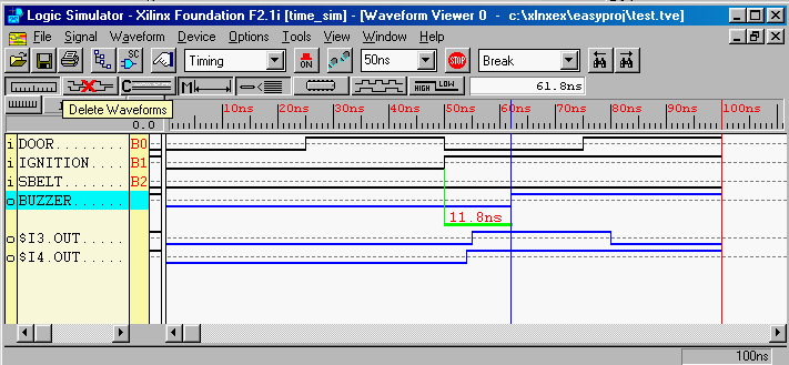
Figure 8: Timing simulation, showing the delay of the output signal
(Buzzer) in relation to the input signal
(Screen clip from Xilinx (TM) Foundation software)
It is instructive to find out what each gate contributes to the delay of the output signal. We have added the output of each gate to the Simulator window as shown in Figure 9. The signal $I8.OUT is the output of the input buf (IBUF), $I6.OUT is the output of the inverter (connected to the DOOR signal), $I3.OUT is the output of the top AND gate and $I5 of the two-input OR gate in Figure 3. These signals can be easily added by going to the SIGNAL -> ADD SIGNAL menu in the Simulator window. This opens the Component selection window, shown in Figure 10. To add the output, for instance, of the 2-input OR gate, click on $I5 - X_or2 in the chip selection column. This will show the input and output signals of the OR gate in the right column (Pins). Double click on the OUT signal to add this signal to the Simulator window. The same can be done for each other logic gate. If you are not sure about the names of the gates, you can go back to the schematic and click on the Query Window icon (left most icon on the top toolbar of the Schematic editor) and point to the gate of interest, shown in Figure 11. If one would have named each net, it would have been more convenient to add each signal to the Simulator window, as was the case for the named input and output nets.
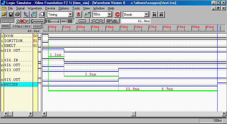
Figure 9: Timing simulation showing the delay associated with each logic
gate. (Screen clip from Xilinx (TM) Foundation software)
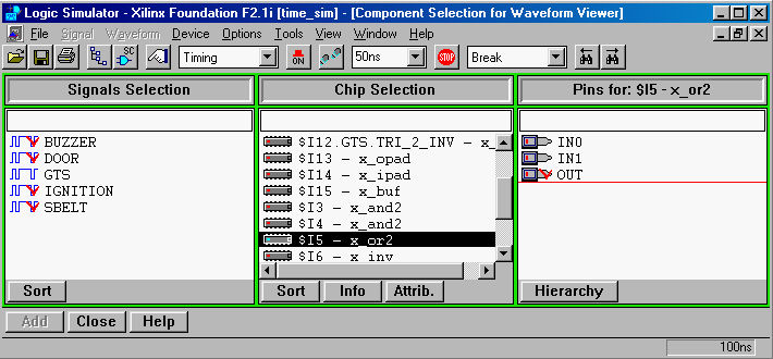
Figure 10: Component selection window. (Screen clip from Xilinx
(TM) Foundation software)
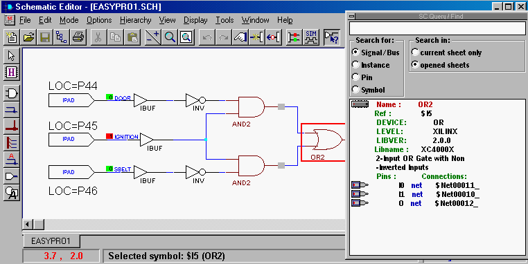
Figure 11: Use of the Query feature in the Schematic editor to find
symbol references for a gate. The Query window on the left
shows that the OR gate is referenced by the name $I5. (Screen clip
from Xilinx (TM) Foundation software)
It is clear from the timing diagram that the total delay of 11.8ns is the result of a delay of 1.1ns through the input buffer (IBUF), 3.8ns through the AND gate and 6.9ns through the output buffer (OBUF). One also notices that there is not delay associated with the inverters or the OR gates. This is because the compiler optimized the circuit and trimmed the inverters. The overall circuit operation is of course the same as the original one but the way it is implemented is different. One should realize that logic circuits are implemented on a FPGA by look-up tables instead of gates. A list of removed logic can be found in the Map report of the Implementation Reports Files.
Script Files
An alternate way to define the waveforms and to run the simulator is to use a Script file. To open the Script editor, go to TOOLS -> SCRIPT EDITOR. A dialog box will open. You can use the Script Editor Wizard which will guide you through the creation of the script file. For more information on how to create a script file, click on the HELP button or go to HELP -> HELP TOPICS in the Srcipt Editor window.
Note on undefined signals when doing a timing simulation:
It is possible that for a complex design some of the signals show up as undefined (a grey box in the Waveform viewer or a blue X on the schematic). This could be due to a couple of reasons. Here are some solutions to this problem.
1. In the Program Manager window, select IMPLEMENTATION -> OPTIONS. In the Options window, click on the Edit Options button for the Simulations Option (Foundation EDIF). In the Simulation Options window, click on the General Tab and De-select the option: Correlate Simulation Data to Input Design as shown in the figure below.
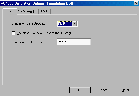
Figure 12: Implementation/Simulation Option window. (Screen clip from Xilinx (TM) Foundation software)
2. Signals which come from one combinational circuit and feed into another one are often placed in the same CLB. Some of these signals are not essential for the operation and the synthesizer may optimize them out. As a result they are not available for timing simulation. You can check which logic has been removed by going to the Map Report (right side window pane - Report tab in the Project Manager window) after doing the implementation. If you want to keep the signal, you can instruct the program to do so. There are two possibilities. One is in the ucf file, as follows: net net_name keep; (in which net_name is the name of the net you do not want to be removed). Another method is by placing the "keep" attribute on the net in the schematic editor:
- double click on the net
- select "attribues"
- in "parameter name", type "keep"
- select "add" (if you like, you can show the attributes)
- then "ok"
Created by Jan Van der Spiegel
<jan@ee.upenn.edu>; August 26, 1997; Updated by Jan Van der Spiegel;
May 17, 2000.
Copyright, J. Van der Spiegel, 2000.