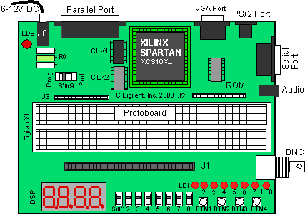
Digilab board (Digilent, Inc.)
i. Board Set-up
A description of the Digilab board is given in the section "Digilent Digilab Board". The board contains a Spartan XCS10XL or XCS05XL FPGA that can be programmed over a parallel cable. Check that the board is powered up and that the switch SW9 is in the PROG position (see Figure below).
Digilab board (Digilent, Inc.)
In the Project Manager window, highlight the design project you want to download and select the desired revision (in the left pane window, Versions tab) as shown in Figure 2 below.
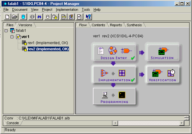
Figure 2: Design Manager window (Screen clip from Xilinx (TM) Foundation
software)
iii. Open the Hardware Debugger
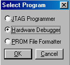
Click on the Programming button in the right window pane (Flow tab)
of the Project Manager. A small Select Program window will pop up: select
the middle button - Hardware Debugger - and click OK.
The Hardware Debugger window will now open, shown in Figure 3 below.
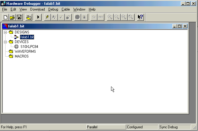
Figure 3: Hardware Debugger window (Screen clip from Xilinx (TM) Foundation software)
iv. Download the bitstream
In the Hardware Debugger window, pull down the CABLE menu and select COMMUNICATIONS. This will bring up the Communications Setup windows shown below. Select the Parallel Cable and click on the OK button.
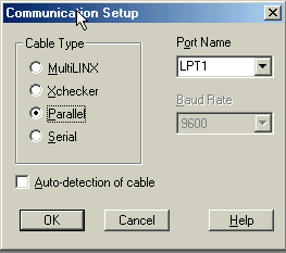
Figure 4: Communications setup window (Screen clip from Xilinx (TM) Foundation software)
Next, select DOWNLOAD menu -> DOWNLOAD DESIGN. This will initiate the downloading of the bit stream. Your device has been programmed. You are now ready to test the design.
Note: If an error occured, double check that the design has been
compiled for the right type of device. The device type for which the design
has been compiled is shown in the Hardware Debugger window. Compare it
with the device on the Digilab board. If the device type does not correspond
to the one on your board, change it by going to the Proejct Manager and
select FILE -> PROJECT TYPE. This will allow you to change the device type.
If you change the type, you need to reimplement the design.
b. Using the Xilinx Demoboard with the XChecker cable
i. Board Set-up
A descirption of the board is given in the section "FPGA
Demonstration Board". The board allows you to program the FPGA with
the XChecker cable. Make sure the demoboard is powered and the XChecker
cable connected properly. The configuration switches SW2 (1 through 8)
should be set as described in the Xilinx FPGA
DemoBoard
write-up (ON - OFF - OFF - ON - ON - ON - ON - OFF). The decimal points
of the two left most 7-segment displays should be "ON" at this point. Figure
1 shows a schematic figure of the demoboard,
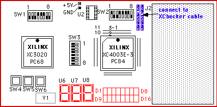
Figure 1: FPGA Demo Board (Ref. Xilinx)
ii. Select project version and revision.
In the Project Manager window, highlight the design project you want
to download and select the desired revision (in the left pane window,
Versions tab) as shown in Figure 2 below.
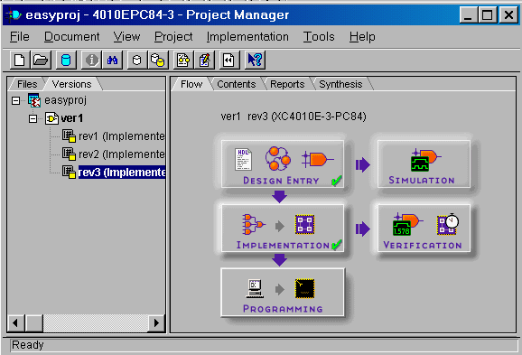
Figure 2: Design Manager window (Screen clip from Xilinx (TM) Foundation software)
iii. Open the Hardware Debugger
Click on the Programming button in the right window pane (Flow tab) of the Project Manager. A small Select Program window will pop up: select the middle button - Hardware Debugger - and click OK.
The Hardware Debugger window will now open, shown in Figure 3 below.
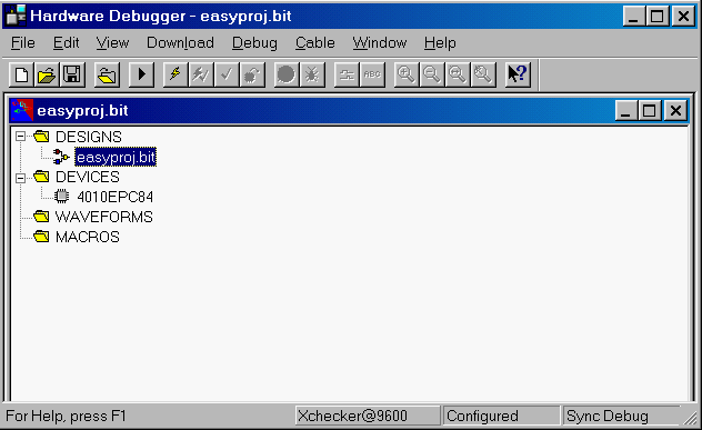
Figure 3: Hardware Debugger window (Screen clip from Xilinx (TM) Foundation
software)
iv. Download the bitstream
In the Hardware Debugger window, select DOWNLOAD menu -> DOWNLOAD DESIGN.
The downloading process should start. During downloading, the decimal point of the right-most 7-segment (U8) display acts as a programming error indicator. During programming the decimal point of U6 and U7 will be lit, while that of U8 should be off. When downloading is successful, the decimal point of U7 will go off and that of U6 stays lit. If a programming error occurs, the decimal point of U8 comes on.
The software will say "DONE signal went high" and will give no errors if the programming was successful. You can now start testing your design.
If an error occurred, check the XChecker cable, the power to the board, and the switch settings. In case there is a problem with the cable, go to the CABLE - > COMMUNICATIONS. In the Communications Setup select: PORT (choose COM1), Cable Type (XChecker), Baud Rate (9600). Also, make sure that the design has been compiled for the right type of device. Check that the device type (go to the Project Manager window and select FILE -> PROJECT TYPE) corresponds to the device on the board. If it is compiled for a device other than XC4010EPC84, choose the right one and re-implement the design.
A description of the XS40 board is given in the section "XS40 Prototyping Board". The board can be used to program the XC4005XL FPGA through the parallel port of a PC or from the on-board EEPROM. The mode of operation depends on the jumper settings, as explained in the XS40 Board description. We will first explain how to use the parallel port to program the device (programming the on-board EEPROM is shown further on).
i. Programming the FPGA on the XS40 board through the parallel port.
Make sure that the jumpers
are in their default configuration so that you can program the board through
the parallel port. We will use the GXSLOAD utility to program the FPGA.
The following steps will download the design from the PC in the FPGA.
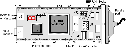
Figure 4: Schematic view of the XS40 board
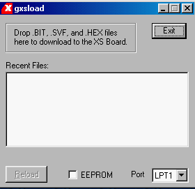
Figure 5: GXSLOAD window for programming the FPGA through the parallel
port.
(Screen clip from the XESS GXSTools).
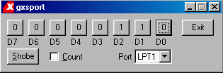
Figure 6: GXSPORT window for applying test signals through the parallel port.
In case you do not have the GXSLOAD program, you can give the load command in a DOS window as follows:
C:\> XSLOAD my_proj.bitYou may have to give the full pathname for your project or change to your project directory before issuing the xsload command. You can use the same command to download an Intel-formatted HEX file into the SRAM on the XS40 board:
C:\> XSLOAD my_file.hex
or
C:\> XSLOAD my_file.hex my_proj.bit
NOTE: you can download the XSTOOLs from the XESS
Corp. website. Once you have saved the xstooset.exe file on your
PC, double click it. The set-up program will create a XSTOOLS\BIN directory
which contains the GXS utitilies to program the FPGA on the XS board (gxsload.exe),
to set the on-board clock (gxssetclk.exe), to test the XS board (gxstest.exe)
and to apply test signals to the board (gxsport.exe).
ii. Storing the configuration file in the EEPROM on the XS40 board
You can also store your design in the on-board non-volatile EEPROM. As soon as you power on the board, the FPGA will be configured from the PROM and is ready to be used, without having to program it from the parallel port. This is convenient once you have finalized your design. In order to store the configuration file on the PROM, you will need to add an EEPROM in socket 7 of the XS40 board and set a few jumpers. Use an AT17C256 Atmel reprogrammable serial EEPROM in the event you want to store the configuration files for the XS4005 or XS4010 FPGAs. Follow these steps to load the design in the Atmel EEPROM.
We will use the GXSLOAD utility to program the CPLD. Make sure that
the jumpers have their default settings as explained in the section "XS95
Prototyping Board".
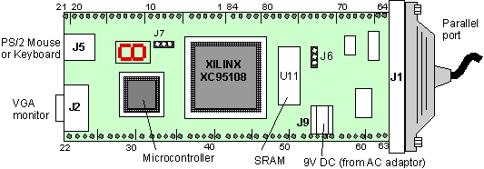
Figure 7: Schematic view of the XS95 board.
Before you can download the bitstream in a CPLD you need to translate the bitstream generated by the Flow Engine into a format that is suitable for the CPLD device. This is an extra step that was not needed for a FPGA. If you haven't done this step yet, do it now. Once you have generated the right file (.svf), download the design (.svf file) from the PC in the CPLD on the XS95 board as follows:.
In case you do not have the GXSLOAD program, you can give the load command in a DOS window as follows:
C:\> XSLOAD my_proj.svfYou may have to give the full pathname for your project or change to your project directory before issuing the xsload command. You can use the same command to download an Intel-formatted HEX file into the SRAM on the XS95 board:
C:\> XSLOAD my_file.hex
or
C:\> XSLOAD my_file.hex XSLOAD my_proj.svf
NOTE: you can download the XSTOOLs from the XESS
Corp. website. Once you have saved the xstooset.exe file on your
PC, double click it. The set-up program will create a XSTOOLS\BIN directory
which contains the GXS utitilies to program the FPGA on the XS board (gxsload.exe),
to set the on-board clock (gxssetclk.exe), to test the XS board (gxstest.exe)
and to apply test signals to the board (gxsport.exe).
Copyright 1999, Jan Van der Spiegel. Created by Jan Van der Spiegel <jan@ee.upenn.edu>; August 27, 1997; Updated August 5, 2001