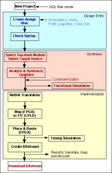
Figure 1: Overview of the design and implementation sequence of a HDL Flow project.
Figure 1: Overview of the design and implementation sequence of a HDL Flow project.
In this tutorial you will learn how to enter and synthesize a VHDL based design. Once you have synthesized the VHDL file, the remaining steps of implementation and downloading will be identical as the ones for the Schematic Flow mode.
i. Open a Project in the Foundation Project Manager
If you are not in the Foundation Project Manager, open it now and create a new project called EasyVHDL. We will create the same logic function as was done before in the Schematic Entry section (circuit of Figure 2). Go to the FILE -> NEW PROJECT menu. In the pop up window, select for flow "HDL". The family and part pull down menus will not be displayed, since you will specify this later during the synthesis process (Figure 1 above).
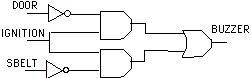
Figure 2: Logic circuit to be implemented as a VHDL file.
ii. Create a VHDL Design and assign port names with the HDL Wizard
In the Foundation Project Manager, click on the HDL Editor icon or go to the TOOLS -> DESIGN ENTRY ->HDL EDITOR menu. Select HDL Design Wizard. In the Design Wizard window click NEXT and go to the Design Wizard Language window. Select VHDL as the design language. Click on NEXT button which will open the Design Wizard Name window. Enter the name of your design. Lets call it EasyVHDL. You can give it another name, but the name should not be larger than 8 characters.
Then click NEXT. The Design Wizard Ports window will appear showing a symbol on the left. Follow the instructions in this window. You can create here the input and output pins (ports). Use the same names as you did for the schematic of Figure 2 (DOOR, IGNITION, SBELT and BUZZER). Click on the NEW button and enter the Name, select as Direction Input or Output, depending on the type of port. For output pins you go to the ADVANCED button which will open the Advanced Port Setting windows. Select STD_LOGIC. When done, click on the FINISH button. The HDL Editor window will open at this point.
iii. Create the Source with the VHDL Editor
The HDL editor window will open a template which contains the Entity
and Architecture section. The Entity section contains the input and output
Port declarations made in the previous step. You should verify that all
the inputs and outputs are present. The Architecture section contains the
logic description of the circuit. Logic descriptions can be entered
in a variety of ways: Equations, Truth Tables, and State Description (for
sequential circuits). We will be using an equation to define the logic
function of Figure 2. Under the Architecture section (<<enter your
statements here>> ) type the following equation:
Figure 3 gives the VHDL source file for the circuit of Figure 2.BUZZER <= IGNITION and (not DOOR or not SBELT);
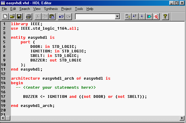
Figure 3: VHDL Editor window for the circuit if Figure 1 (Screen clip from Xilinx (TM) Foundation software)
To find out more about the VHDL syntax click on the Language Assistant icon on the top right the toolbar, or select TOOLS -> LANGUAGE ASSISTANT. This will bring up a window with language and synthesis templates. The language templates shows basic language constructs while the synthesis templates give the code of functional blocks such as counters, multiplexers, adders, flip-flops and architectures features such as Boundary Scan and RAM blocks. Figure 4 shows the Language Assistant window.
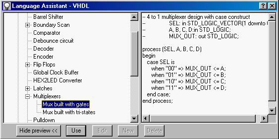
Figure 4: VHDL Language Assistant window showing the template for a
multiplexer. (Screen clip from Xilinx (TM) Foundation software)
iv. Check Syntax
Lets make sure no syntax errors have been made. Go to the SYNTHESIS -> CHECK SYNTAX menu. If successful, a pop-up window will show "Check Successful". Also, the bottom window pane in the Project Manager will display a status of the process or report any errors. To learn more about the errors, open the synthesis report (SYNTHESIS -> VIEW REPORT in the HDL Editor window).
v. Add the design to the Project
To make the HDL source file part of the Project go to the PROJECT
-> ADD TO PROJECT menu in the HDL Editor window. The
easyvhdl.vhd file should now appear in the Project Directory on the Project
Manager Window (Files tab). You can now exit the HDL editor. You will notice
that the right window pane in the Project Manager shows an additional icon
for the Synthesis operation (Figure 5). In case you want to create a macro,
select PROJECT -> CREATE MACRO (see section on Macros
and Hierarchical designs)
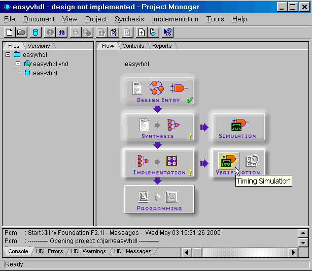
Figure 5: Project Manager for the HDL flow mode. (Screen clip from
Xilinx (TM) Foundation software)
vi. Analyzing and Synthesizing the Design
First you will analyze the syntax by going to SYNTHESIS -> ANALYZE ALL
SOURCES menu in the Project Manager window. To view warnings or errors
click on the HDL Errors, Warnings of Messages Tab at the bottom of the
Project Manager. When the files have been successfully analyzed you can
translate the design into gates, optimized for the target device.
References:
Created by Jan Van der Spiegel;
August 26, 1997; Updated by Jan Van der Spiegel May 16, 2000.
<jan@ee.upenn.edu>;