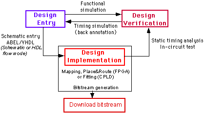
Figure 1: Overview of the Design Flow.
Figure 1: Overview of the Design Flow.
Go back to the Project Flowchart in the Project Manager window. If this is the first time you implement the design, click on the Implementation icon in the flow section of the Project Manager window. This will open the Implement Design window, shown in Fig. 2 below. If you have implemented earlier an earlier version and would like to create a new revision or new version, go to the PROJECT -> CREATE REVISION or CREATE VERSION menu. This will open the Create Revision or Version window, similar to the Implement Design window shown in Fig. 2. The Implement Design Window lets you specify the target device and speed grade. In case you get a message saying "Schematic Netlist is older than the Schematic. Update netlist from Schematic Editor?", click the YES button. The target device is already specified as 4005XLPC84 as this is the one we selected when the project was created. If needed, you can change the target device. The Revision and Version name is automatically filled in with rev1 and ver1. You can change the name if you want to. The implementation options allow you to specify how the design is optimized, mapped, placed, routed and configured. In general, the default settings should be good enough for introductory lab exercises. When you click on the SET button, the Settings dialog box will open. This allows you to specify control files such as a specific Constraint, Guide or Floorplan files. The default settings are usually fine. In case you are using the HDL Flow mode for your project, the Implementation Settings window will open. Click on the RUN button to start the implementation process.
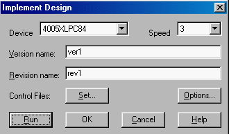
Figure 2: Implement Design Window (Screen clip from Xilinx (TM) Foundation software)
Note: If you need to switch to another device family, you can do so by going to the FILE -> DEVICE TYPE menu in the Project Manager window. The change Project Type window will pop up. Under Flow, select the new device type (ex. XC9500 in case want to switch to a CPLD device).
When you click on the RUN button in the Implement Design window,
the Flow Engine window will open and display the progress through the different
steps in the implementation process. Figure 3 shows the Flow Engine window
in case the target device is a FPGA.
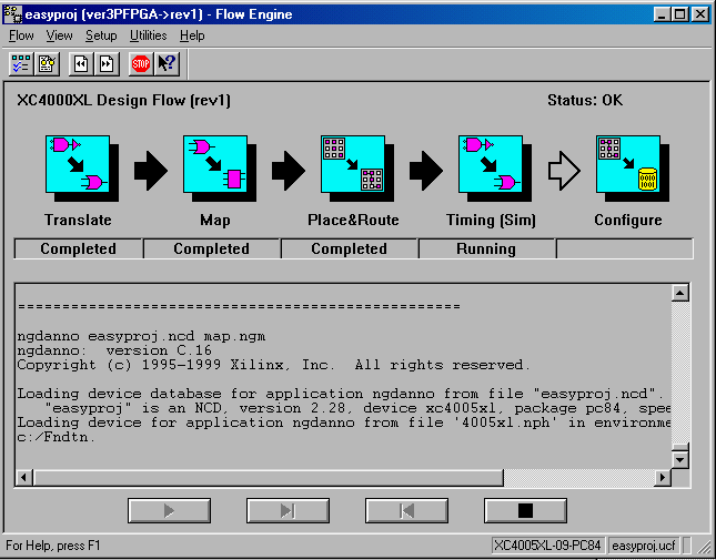
Figure 3: Flow Engine window for a FPGA target device (Screen clip from Xilinx (TM) Foundation software)
The first step is the translation of the design file (EDIF file) in a proper format (NGD file - Native Generic Database). This implies that the representation of your schematic (gates) or HDL file is translated into FPGA elements corresponding to the target device (look-up tables, etc). The next step is mapping of the design to the specific target device. The mapper optimizes the logic, trims or "optimizes out" (removes) logic and maps the design in the targetted FPGA device. Next is the Place&Route operation, followed by the generation of the timing information for use by the timing simulator. The final step is the generation of the Bitstream which is a configuration file that can be used to program the FPGA. In case you want to program a PROM, you will run the bitstream through the PROM File Formatter. You can follow the status of each step in the Flow Engine window.
When the implementation is complete a small window will pop up informing you that the Flow Engine is Completed Successfully. Click OK. In case errors occurred you should refer to Implementation Log file, in the Project Manager (click on the Reports tap on top of the right window pane), as shown in Figure 4 below. In the hierarchy browser (left pane window) of the Project Manager, click on the Versions tab and you will see the status of the implementation.
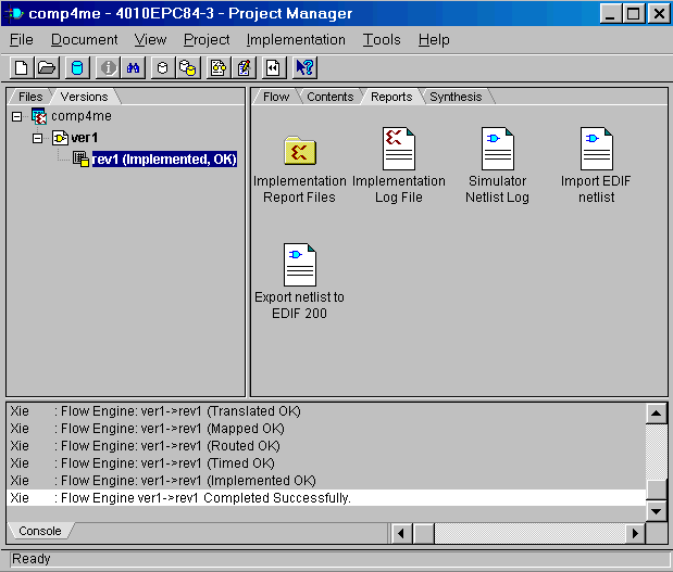
Figure 4: Project Manager showing the status of the implemented version
and the reports. (Screen clip from Xilinx (TM) Foundation software)
In case you are targeting the design for a CPLD device, the Flow Engine looks like the one in Figure 5. The bitstream generates a .jed file..
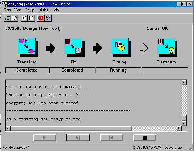
Figure 5: Flow Engine window for a CPLD device. (Screen clip from Xilinx (TM) Foundation software)
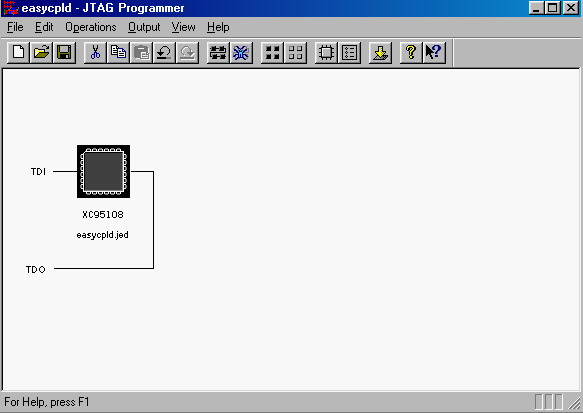
For a CPLD the .jed (bitstream) needs to be first tranlsated into a format that is compatible with the CPLD device before it can be downloaded. This is done as follows.
b. Viewing the Implementation Results
You can also view the reports from the Project Manager (Fig. 4). Reports are associated with each version. In the Project Manager, click on the Versions tab in the left-hand pane. Select the version and revision for which you would like to see the reports. You can then click on the Report Browser icon on the top toolbar. Or you can also click on the Reports tab in the right-hand window pane. Next, double click on the Implementation Report Files. This will open the report browser window. In case you are using a FPGA target device, you will see the Translation, Map, Place&Route, Pad reports and others. Click on the Pad report to see the assignments of the I/O pins. You will recognize the same names as the ones you specified on the schematic (Door, Ignition, Sbelt and Buzzer). Check the pin locations. Another interesting report is the Map report which will tell you if logic has been removed (as part of the optimization) or added. The Place&Route report indicates how much of the device has been utilized. It gives also a rough estimate of the average interconnection delay.
In case you have implemented your design on a CPLD the Translation, Fitting and Post Layout Timing reports will be generated. Open the Fitting report to check the pin locations of the input and output signals.
c. Constraint Files: Assigning pins with the user constraint files: Constraint Editor
There are two types of constraints: (1) location and (2) timing. In general location constraints allow you to control mapping and positioning of logic elements in the target device, such as the location of the pads (I/O pins). Timing constraints inform the system which paths are critical and need short interconnections (high speed lines) in order to ensure that your design's performance functions properly under worst-case conditions. You can also specify the slew rate (fast or slow) and to use pullup or pulldown resistors for the output pads. We will concentrate on the location constraints. More information can be found from the HELP -> FOUNDATION HELP CONTENTS: Entering Constraints.
Constraints can be entered in various ways. One way is to place constraints on the schematic or in the ABEL file, as we have done with the pin location. Other ways are to use the Constraint Editor or edit the user constraint file (projectname.ucf) directly.
Constraint Editor
If you did not assign pin numbers to the input and outputs in your
schematic (or HDL code), you should do it now, before compiling the design.
If you don't assign the pins, the compiler will assign them for you. When
using theDigilab, Demoboard, or the XC40 or XC95 boards you should
assign the pins yourself to make use of the on board switches and LEDs
on theDigilab board, FPGA
demoboard, or the XS40
and XS95 boards.
The Constraint Editor is a Graphical User Interface that you run after the translate program. Notice that you can access the Constraint Editor only after you have created a version of the project and thus after running the tranlation once. Using the constraint editor can be a littel confusing in particular when you have created different versions. You need to make sure that you are editing and using the right constraint file. Follow the instructions carefully:
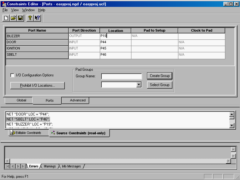
Figure 7: Constraint Editor window (Screen clip from Xilinx (TM) Foundation software)
When you create a new version or revision a window like the one
in Figure 2 will pop up. To make sure you are
using the right user constraint file, click on the SET button. When the
Settings window opens, you can select the desired user constraint file
(ucf) by using the pull-down box for the "Use contraint file from"
menu (see Figure 8). Use "custom" to browse
the directory. If you do not specify a ucf file, the one corresponding
to the last revision will be used.
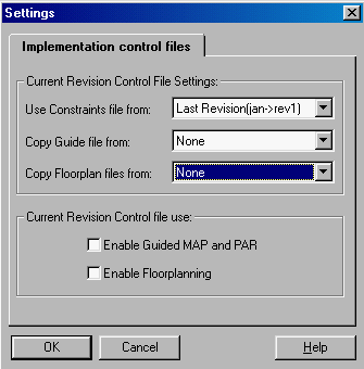
Figure 8: Setting window that allows you to specify a specific user
constraint file.
(Screen clip from Xilinx (TM) Foundation software)
You can also use the Constraint Editor to specify whether an output should have a Pullup or Pulldown resistor, and have a Slow or Fast slew rate. You can specify these by clicking on the I/O Configuration Option box. This will add a few columns to the Ports window. You can now specify the Slew Rate and Pullup/Pulldown option using the pull down menus in the corresponding colums.
Edit the User Constraint File
An alternative way to specify constraints is to edit the user constraint
file directly after you have run the translate program once. This file
has the same name as the project with a .ucf extension. The easiest way
to edit the .ucf file is by using the HDL editor, by clicking on the HDL
Editor icon in the Project Manager, or by going to TOOLS -> DESIGN ENTRY
-> HDL EDITOR menu. Select "Open Existing Document". The user constraint
file is located in the xproj folder, inside the corresponding version/revision
folder (xproj/ver#/rev#/project.ucf). You will notice that the existing
.ucf file contains a lot of comments (lines starting with #) explaining
how to create a constraint file. Right now we are interested in defining
pin locations. Scroll to the bottom of the file and add the pin locations
as follows.
Be careful - the constraint file is case sensitive. Make sure you use exactly the same name in the constraint file as the one you have defined in your schematic or in the HDL file. The "#" is used for comments. When done, save the file. You can now re-run the implementation tools by selecting the version in the left window pane (versions tab) of the Project Manager. Click on the version with the right mouse button and select "Invoke Interactive Flow Engine". Start the Flow Engine. When finished successful, check the Pad or Fitting report to make sure that the right pin locations have been assigned.NET "BUZZER" LOC = "P19"; # output: DOORNET "DOOR" LOC = "P44"; # inputNET "IGNITION" LOC = "P45"; # inputNET "SBELT" LOC = "P46"; # input
d. Create Design Version and Implementation version
If you want to create a new version or new revision, go to the Project Manager. Select PROJECT -> CREATE VERSION or CREATE REVISION. This will bring up the Create Version or the Create Revision window. These windows look similar to the Implement window discussed earlier. You can specify which constraint file to use by clicking on the SET button next to Control File. Use the pull down menu to select a contraint file from a previous version/revision, as shown in Figure 8. If you do not specify a constraint file it will use the constraint file of the last revision. The versions will appear in the left hand window pane of the Project manager, under the Version tab. Once a new version or revision has been created you can run the implemenation program.
You can use the FPGA Editor to look how the device's resources have been use and placed on the FPGA. You can also use this application to place and route critical components before running the automatic place and route tools on your design. To open the FPGA editor, go to the Project Manager, and select TOOLS -> IMPLEMENTATION -> FPGA EDITOR.
The Editor allows you to display different levels of details on the
FPGA such as short wires, long wires, switch boxes, routing between components,
components, etc. The level of detail that is displayed can be controlled
by clicking icons on the top level toolbar. Figure 9 shows the FPGA editor
window with a view of the FPGA floorplan, around the area where the logic
circuit has been placed. The three blue boxes are the I/O blocks of the
DOOR, IGNITION and SBELT signals, and the red one is the logic block. The
switching network and the routing of the signals to the logic block are
shown as well.
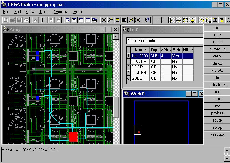
Figure 9: FPGA Editor window with view of the floorplan for the logic
circuit of Fig.1 (Schematic
Entry section).
(Screen clip from Xilinx (TM) Foundation software)
To look at a particular block on the FPGA, you can zoom in by clicking on the maginifying glass on the top toolbar. The bottom left window, labeled World shows a red dot that correspond to the signal that you selected in the List window on top. By moving the white rectangle and placing it on top of the desired signal (red dot) you can zoom into the specific block in the left window, shown as a red rectangle. You can now double click on the red block in the left window to see more details of the selected component.
For more information about the FPGA Editor, select HELP -> HELP TOPICS from the FPGA Editor window.
In case you are implementing your design on a CPLD, you can use the Chip Viewer to see how the resource inside the CPLD has been used. The ChipViewer tool allows you to examine inputs and outputs, macrocell details, equations, and pin assignments. You can examine both pre-fitting and post-fitting results. To start the tool, go to TOOLS -> IMPLEMENTATION -> CPLD CHIP VIEWER in the Project Manager window. For additional information go to the HELP -> HELP TOPICS menu in the Chip Viewer window.
References:
Created by Jan Van der Spiegel
<jan@ee.upenn.edu>;
August 26, 1997; Updated by Jan Van der Spiegel; June 8, 2000.
Copyright J. Van der Spiegel, 2000.