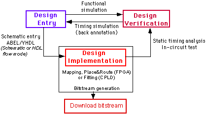
Figure 1: Design flow overview [1]
This write-up is intended to get you started with the Foundation tools. It gives a quick overview of how to create a design, simulate it and download it into a FPGA or CPLD. For more detailed information please consult the on-line XILINX documentation and tutorials. The Foundation 2.1i User Guide is available on line.
Figure 1: Design flow overview [1]
Designs can be entered in two basic modes: Schematic and HDL (Hardware Description Language) mode. A hardware description language allows you to describe the behaviour of a system rather than as individual gates. There are several popular hardware description languages such as VHDL, Verilog and ABEL.
The schematic flow mode allows you to create a design that consists of either a top-level schematic or top-level ABEL file. It can contain underlying schematic diagrams, state machine macros, instantiated HDL (ABEL, VHDL or Verilog) macros, LogiBLOX, CORE Generator modules.
The HDL flow mode can contain a VHDL (or Verilog) or a schematic top-level design with underlying VHDL, Verilog, schematic modules, as well as LogiBLOX, CORE Generator and Finite State Machine modules. Notice that for a top level ABEL-based design, you will need to use the Schematic mode. In order to create VHDL or Verilog designs you will need the Synopsis FPGA Express package which comes with the Foundation Base Express and Foundation Express tools. Figures 2 and 3 show a more detailed view of the different steps involved in the creation of a design in the schematic flow mode and HDL flow mode, respectively. Notice the extra Synthesis step that is required in case of a HDL flow design. Also, the target device and the top-level module is specified during the synthesis step in the HDL flow mode.
The implementation tools fit the entered design into the target device architecture. The tools compile a design file into a configuration file that is optimized in terms of use of logic gates and interconnections for the targeted device. Downloading of the bitstream can be done easily from a PC into a FPGA (using the Xilinx demoboard, the XS40 or XSV boards) or into a CPLD (on the XS95 board). Both devices can also be programmed in-the-system (ISP) by connecting a JTAG or XChecker cable to the device's programming pins.
Design verification includes functional simulation, in-circuit testing,
and timing simulation. Functional simulation can be done after the design
entry to verify the proper operation of the circuit. However, functional
simulation does not provide timing information, such as delays, race condition,
set-up and hold-time violations. This information is obtained from the
static timing simulator and is done after the design has been compiled
for the target device. Figure 2 shows the design
flow for a Schematic Flow project.
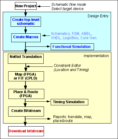
Figure 2: Overview of the design and implementation sequence of a Schematic
Flow project. [2]
Figure 3 shows the design flow for a HDL Flow project. The top-level module and the target device aren't specified until the Synthesis step as shown in the figure below.
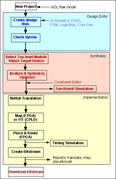
Figure 3: Overview of the design and implementation sequence of a HDL Flow project. [2].
The devices come in a variety of packages. The ones used on the FPGA
demoboard or the XS40 and XS95 boards are packaged in an 84 pin PLCC and
have the following part names: XC4010EPC84, XC4005XLPC84 and XC95108PC84
. To find out which device you will be using, check the board you have
available in the lab. Detailed information on these devices is given in
the Xilinx Programmable Logic Data
Book. The pin outs of the XC4000
and the XC9500 84-pin devices are
available on the tutorial webpage.
You can launch the Xilinx Project Manager by going to the START/PROGRAMS/Xilinx
Foundation Series 2.1i menu. You can also click on the Project Manager
icon at the bottom toolbar. ![]()
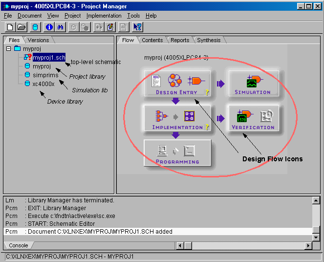
Figure 4: Project Manager showing the Schematic Flow mode. (Screen clip from Xilinx (TM) Foundation software)
When you create a new project e.g. MyProj, the Foundation tools will create the following files: a project configuration file (PDF), called Project Description File (myproj.pdf), and three library files, the project library file (myproj), the simulation library file (simprims) and the device library (xc4000x) files. The libraries are shown in the left window pane (called the Hierarchy browser) of the Project Manager. A project must always have one or more top level design files. In case the top-level cell is a schematic, the file will be shown in the hierarchy browser with an extension .sch (e.g. myproj.sch) as can be seen in Figure 4 above. The foundation tools will create additional folders and files during different stages of the project design/implementation.
The right window pane in the Project Manager has several tabs. The Flow tab graphically shows the different steps involved in the design of a project as was shown schematically in Figure 2. You can click on the icons to access a particular tool as will be shown later on.
The bottom window pane gives status and error or warning messages. The different features of the Project Manager will become clear later on when doing the tutorial exercises. For more information, go to the HELP -> PROJECT MANAGER HELP TOPICS menu.
In case a library is missing (e.g. the device library), the tools will
give you a warning. This will also show up when you try to open the schematic,
as symbols will be missing or blanked out. If that happens, you can add
the library to the project. In the Project Manager, go to FILE ->PROJECT
LIBRARIES. This will open the Project Libraries window, shown in Figure
5. The left side panel shows the "Attached Libraries" and the right side
windows the Project Libraries, such as myproj, xc4000x and simprims. If
any of these are missing, you can add them from the list in the left side
window. Scroll until you find the right library (e.g. XC4000X) and click
the ADD button.
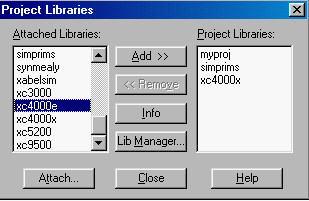
Figure 5: Project Libraries window. (Screen clip from Xilinx (TM) Foundation
software)
If the required library does not show up in the left side window, you need to attach the library first. Click the Lib Manager button to open the Library Manager. Go to the LIBRARY -> ATTACH menu to open the Attach Library. You can now select the required library and click the OK button. The systems' libraries are usually found in the c:\fndtn\active\syslib directory. The newly selected library will appear in Attached Library list. You can now add the library to your project. Notice that libraries which are already attached will not be displayed in the Libraries list.
References
Created by Jan Van der Spiegel<jan@ee.upenn.edu>; August 26, 1997; Updated by Jan Van der Spiegel; May 30, 2000.