Digital Design Laboratory
Implementation of a 4-bit Adder with
7-segment HDL decoder
and the use of the
VHDL Hardware Description Language (HDL)
Purpose:
The purpose of this lab is:
-
1. To get familiar with the basics of a hardware description language.
-
2. To design a decoder for a 7-segment display as part of the 4-bit adder.
-
3. Implement the design and configure the FPGA or CPLD.
-
4. Experimentally verify the operation of the 4-bit adder and display the
result on two 7-segment displays.
Note: You will be using the Digilab board for the
implementation and the VHDL Hardware description language for high
level circuit descriptions.
Pre-lab assignments:
The pre-lab section consists of two parts, each having its own set of
pre-lab questions. This lab is more extensive than the previous lab.
Make sure that you do all the readings and answer all questions before
coming to the lab or you will not be able to finish it on time.
DECODER
In the previous lab you designed a 4-bit adder (MY4ADD) using a full
adder (MYFA) as a building block. In this lab you will be expanding the
circuit to include a decoder (designed in HDL) so that you can display
the results of the addition on a 7-segment display. The block diagram of
the system is given in Figure 1. At the end of the lab, you will implement
this adder in an actual PLD (FPGA or CPLD) and experimentally verify the
performance.
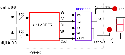
Figure 1: Schematic block diagram of the 4-bit adder system. The 7-segment
LED for
the tens digit is not available on the XS40 or XS95 board.
The project involves the design of a display decoder that decodes a
5-bit
binary number coming from the 4-bit adder (four Sum bits and one Carry_out
bit) and which displays the results on a 7-segment LED display. If you
are using the Digilab board and FPGA demoboard, you have two 7-segment
displays available (one for the digits and one for the tens). However,
the XS40 and XS95 boards have only one 7-segment display. In that case
you won't be able to display numbers larger than 9, unless you add an additional
external LED for the ten digits (more about this during the implementation
and testing steps). The decoder circuit is somewhat different from
a regular 7-segment display decoder which decodes a BCD input (i.e. a 4-bit
binary word) to display the results on a single 7-segment display.
The block diagram of the decoder is shown in Figure
2.
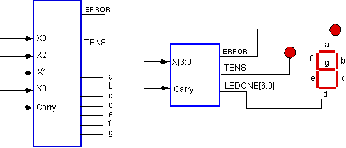
a.
b.
Figure 2: Block Diagram of the 5-bit decoder circuit: (a) detailed
and (b) simplified block diagram.
The inputs to the decoder are Carry and X3, X2, X1, X0 (for short
[X3..X0] or X[3:0]) and the outputs are a1, b1, ..., g1; and tens corresponding
to seven signals for the units 7-segment display and the tens digit.
In order to design this circuit you will need to come up with the truth
table. In doing so, remember that the two 4-bit input words that need to
be added each represents a digit (from 0 to 9 as in a BCD code) and thus
can have a maximum value of 9 each (or 10012). The largest
number that needs to be displayed is thus 18, which occurs when the two
4-bit inputs of the adder are both 9. As a result, the truth table has
only 19 entries, starting from 00000 to 100102. This will simplify
the design of the decoder considerably because any signal larger than 18
(or 100102) is not possible. If it were to occur, we know an
error must have occurred during the operation, or that we added numbers
larger than 9 (which is not allowed if we use a BCD representation). The
digit of the tens can only be 0 or 1.
-
When using VHDL, read the following sections of the VHDL
Primer.
-
When using ABEL, read the following sections of the ABEL-HDL
Primer.
-
1. Introduction
-
2. Basic Structure of an ABEL source file
-
3. Declarations
-
4. Numbers
-
5. Sets (only the introduction section; you can skip section 5a and 5b)
-
6. Operators
-
7. Logic Description: sections a and b only
-
10. Miscellaneous: section a.
-
Read also the tutorial on "Entering
a Design with VHDL" or "Entering
a Design with ABEL-HDL", depending on the language of choice.
- Pre-lab Questions (part 1 of 3 - 10 pts.) (Use Blackboard
to submit your answers online; first write them down in your lab notebook
since you will need them to do the lab).
-
Generate the truth table for units digit (least significant digit). This
table has as inputs Carry, X3, X2, X1, X0 and as outputs the seven segments
a, b, c, d, e, f, g. As was discussed in the description of the Digilab
board, the LEDs of the 7-segment
displays will light up when a low signal ("0") is applied to its cathode.
Thus the signals of these segments should be realized as "ACTIVE-LOW" (making
the function "a" equal to "0" will light the LED up).
-
For the tens digit, we know that it can only be blank (0) or 1. The output
should be digit 1 as soon as the result of the addition is 1010
(=010102) or larger. Find the logic expression for the TENS
digit and write it as a minimized sum of product expression. (note the
signal TENS can be an expressed as an active-high signal, since we
will display it on a regular LED).
-
Derive and give the logic equation for the ERROR signal that goes ON whenever
the output is larger than 18. Since this ERROR signal will be displayed
on one of the regular LEDs, this signal is an active-high signal.
-
Pre-lab Questions (part 2 of 3 - 10 pts.) related to VHDL.
IMPLEMENTATION
You will implement your design on a FPGA or CPLD which will complete
the design
cycle as explained in the introduction of the Foundation tutorial.
Configuring and testing your design will be done using one
of the prototyping boards. These boards contain the device (FPGA or CPLD)
together with a series of switches, 7-segments displays, LEDs as well as
power connections. It will be important for you to get familiar with the
major features of the board your are using.
-
Getting yourself familiar with the board
-
If you are using the Digilab board, read the description
of the board (up to the section "Seven-segment display").
-
Use the General Purpose Switches SW1-SW8 to apply inputs to the adder.
Use the first 4 switches for the A (A3..A0) and the last four switches
of the B inputs. The pin numbers to which the switches are connected are
given in the table in the section describing the switches
SW1-SW8.
-
Use seven-segment
displays DISPL 4 for the least significant digit (units). Consult
the
table with
the pin numbers corresponding to the different segments of the displays.
To use the display, the cathodes of the individual segments (A, B,
C, ...G) need to be connected to the signal one wants to display. When
the signal on the cathode is "High" the segment will be OFF and when the
signal is "Low", the segment will light up. Thus the signals that drive
the seven-segment display are "Active-Low".
-
For the TENS digit, you can use can use one of the
regular LEDs on the Digilab board (e.g. use LD1).
-
For the ERROR signal use LED LD8. Check the Digilab description ( table)
to find out to which pins of the FPGA these LEDs are connected.
-
The other connections to the FPGA such as Vdd (Power), Ground, Programming
and mode pins, etc., are already made on the board. So you do not need
to concern yourself about it.
-
If you are using the FPGA demoboard, read the description
of the board (sections up to LED bar indicators). The board houses
two types of FPGAs: XC4010E (or XC4003E) and XC3020A. You will be using
the XC4010E (or XC4003E - check the FPGA on the board).
-
The General Purpose Switches SW3 can be used to apply inputs to your adder.
There are 8 switches, so you can use the first 4 switches for the A (A3..A0)
and the last four switches of the B inputs. The pin numbers to which the
switches are connected are given in the table in the section describing
the switches
SW3.
-
The 7-segment displays are described in the "7-segment Display" Section
together with the pin numbers to which they are connected. Consult the
table
for pin numbers. Use segments "b" and "c" of U7 for the most
significant digit (it can only be blank or 1) and U8 for the least significant
one. Notice that the LEDs will go on when the signal applied to it is low
(i.e. the LEDs are "active-low").
-
For the ERROR signal you can use one of the 8 LEDs of the Bar Indicators.
Check the demoboard description ( table)
to find out to which pins of the FPGA these LEDs are connected.
-
The other connections to the FPGA such as Vdd (Power), Ground, Programming
and mode pins, etc., are already made on the board. So you do not need
to concern yourself about it.
-
If you are using the XS40 board, read the general introduction
of the board, and the sections on the 7-segment LEDs and parallel port.
-
This board has one 7-segment LED display that allows you to show one digit.
The pin numbers
of each segment are given in the write-up. The LEDs will light up
when a "high" signal is applied over its terminal and will go off when
a "low signal" is applied. These LEDs are thus "Active-high".
-
Input signals can be applied through the parallel
port.
-
In case you are using the XS95 board, get yourself familiar with
its main features. Read the general introduction,
and the sections on the 7-segment LEDs and parallel port.
-
This board has one 7-segment LED display that allows you to show one digit.
The pin numbers
of each segment are given in the write-up. The LEDs will light up
when a "high" signal is applied over its terminal and will go off when
a "low signal" is applied. These LEDs are thus "Active-high".
-
Input signals can be applied through the parallel
port.
-
Read the tutorial on "Implementation".
This section deals with translating, place&routing, and mapping or
fitting (CPLD) the design. The result of the implementation process is
a bitstream that can be downloaded for programming the device.
-
Assigning pin numbers. Once you are
familiar with the prototyping board and its connections you should make
a table with the names of the input and output signals (as indicated on
your schematic MY4ADD). The names of the signals should be identical to
the ones you used to name the nets of the input and output pads (see your
schematic of the 4-bit adder with decoder). These include the 8 inputs
for A3..A0, B3..B0, the 7 outputs for cathodes of the 7-segment display
A, B, ... G, the TENS and the ERROR signals. Make a table
with the pin names and corresponding pin number to which you want
to connect each signal. The pin numbers will depend on the type of board
you are using.
-
For the Digilab board, the input A3 input should be connected
to switch SW1, A2 to SW2, A1 to SW3 and A0
to SW4 in this sequence; B3 should be connected to SW5, B2
to SW6,... B0 to switch SW8. From the Digilab board description
(table of
the switches) you will find that SW1 is connected to pin 28 of the
FPGA, etc . The output of segment "A" should be connected to the cathode
of segment "A" of the 7-segment
display, which corresponds to pin number 51. Do the same for all inputs
and outputs. For the ERROR signal use LED8. Write the table down in your
lab notebook; you will need it later in the lab. You will also fill
out a similar table as part of the online quiz (see next).
-
For the XS40 board, you have only one 7-segment display available.
This will be used to display the unit digit. The output D1A should thus
be connected to segment "a" of the 7-segment
LED, which corresponds to pin number 19; output D1B to pin 23, etc.
The inputs A and B will be applied through the parallel port. Connect A1
to parallel port D0, A2 to D1, ..., B1 to D4, etc. You will find that D0,
D1,... is connected to pins 44, 45, etc. The pins 32 and 34 which are connected
to the parallel ports D6 and D7 on the XS40 board are special purpose pins
used by the FPGA to set the mode at power up: M0 and M2 pins. In
order to assign input signals to these pins you will have to place special
pad symbols on the schematic instead of the regular IPADs: use MD0 and
MD2 pad symbols. By using these symbols the signal will be automatically
connected to the pin number 32 and 34, respectively.
-
For the FPGA demoboard, the A0 input should be connected to switch
SW3-1, A1 to SW3-2, in this sequence. From the Demoboard description (table
of SW3) you will find that SW3-1 is connected to pin 19 of the XC4010E.
The output D1A should be connected to segment "a" of the 7-segment
LED U8, which corresponds to pin number 49. Do the same for all inputs
and outputs. The tens digit can only have the value 1 or 0 and thus needs
to be connected to segments "b" and "c" of the LED display. Write the table
down in your lab notebook, because you will need it later in the lab. Take
into account that you will need active-low signals to drive the LEDs. For
the ERROR signal use one of the bar LEDs. You will also fill out a similar
table as part of the online quiz (see next).
-
For the XS95 board, you only have one 7-segment display available.
This will be used to display the unit digit. The output D1A should thus
be connected to segment "a" of the 7-segment
LED, which corresponds to pin number 15; output D1B to pin 18, etc.
You can use the decimal point to indicate the tens digit. Inputs A and
B will be applied through the parallel port. Connect A1 to parallel port
D0, A2 to D1, ..., B1 to D4, etc. You will find that D0, D1,... is connected
to pins 46, 47, etc.
-
Read the tutorial on "Configuring
a Device". This section explains how to download the bitstream in the
target device. Read the section corresponding to your prototyping board.
For the XS40 board, read only the section on "Programming
the FPGA through the Parallel Port"
- Pre-lab Question (part 3 of 3 - 5pts) (Use Blackboard
to submit your answers online; first write them down in your lab notebook
since you will need them later to do the lab).
-
Fill out a table (on Blackboard) with the pin numbers of the input and output
signals (see the section above on Assigning pin numbers).
In-lab assignment:
A. Parts and Equipment:
-
PC
-
Xilinx Foundation Tools F2.1i
-
FPGA board (Digilab, XS40 or FPGA demoboard)
B. Experiments
The lab consists of two parts. The first part is to design
the decoder (as a macro). The second part is to add the decoder to the
existing 4-bit adder (MY4ADD) schematic and simulate the overall system.
1. HDL Source file for the DECODER:
General Information.
Write the HDL source file for the decoder circuit you designed
as part of the pre-lab (Figure 2). In case you work with VHDL, you can use the
"WITH-SELECT-WHEN" construct to specify a truth table (a truth table construct
does not exist in VHDL - consult a VHDL
tutorial or Language assistant for more information). When using ABEL you
can use the Truth Table
option for the units digit, and use the equation
option for the tens digit.
Name the inputs X3, X2, X1, X0 and Carry; for the outputs name them
LEDONE6, LEDONE5, ..., LEDONE0, TENS, and ERROR for the units display,
tens and error signals, respectively. It will be convenient to define the
inputs and outputs as buses X[3:0] and LEDONE[6:0], as schematically shown
in
Figure 2b.
Macro symbol and source file for the Decoder Circuit
-
Start the Xilinx Foundation Tools. Open your project (MY4ADD) of the previous
lab (4-bit adder). When you copy your project from another computer
or disk,
make sure you copy both the project folder
(MY4ADD) AND the .pdf file (my4add.pdf) into your folder c:\users\your_name\.
The .pdf file is required and contains information about the project. Never
place the project inside a folder
whose name has more than 8 characters!
This will give unexpected problems. The best method is to put the project
in a folder with the same name (probably your name) as it was last week.
If you have problems, consult the log file at the bottom
of the Project Manager window or read the "Common
Mistakes" section.
-
Open the schematic editor. This should bring up the schematic of
last lab (4-bit adder circuit).
-
Next you will create the symbol for the macro:
-
In the Schematic Editor window select TOOLS -> SYMBOL WIZARD. Click NEXT.
-
In the Design Wizard Contents window, enter the Symbol Name: MY7DSPL.
-
In the Contents window, select the HDL radio button and VHDL language button.
Then click NEXT.
-
In the Design Wizard Ports window, click on the NEW button to enter the
name of the inputs and outputs. Enter Carry in the name field and select
Input
in the Direction field. Next define the input bus X[3:0]. Click on the
NEW button and enter X[3:0] in the name field and select Input in
the Direction field. Click NEW and enter LEDONE[6:0] in the Name field;
select Output in the Direction section. Before clicking NEW go to
the ADVANCED button and select the 'combination' port when using ABEL or
STD_LOGIC_VECTOR in VHDL. Also include the TENS and ERROR output
port. When finished defining input and outputs, click on NEXT.
-
In the Attributes window, add some comments. When done, press the NEXT
button.
-
Click on the FINISH button. The new symbol will be placed in the project
library.
-
In the Schematic Editor window, place the newly created macro MY7DSPL on
the schematic. Select the hierarchy icon "H" to open the macro. This will
open the HDL editor window. You can now define the new macro for which
you just created the MY7DSPL symbol.
-
You will notice in the Editor window that the pins have already been declared.
Make sure that the output pin LEDONE6.. LEDONE0 have been declared properly
(in ABEL: as an
istype 'com').
-
Enter the equation for the "TENS" digit. Enter here also the equation for
the ERROR signal.
-
For the segments a1, b1, etc, use the Truth
Table construct in ABEL or the"With-Select-When"
construct in VHDL. (for the syntax consult the ABEL primer - section on
LOGIC description, or the VHDL Primer
- section on Dataflow modeling). You can use SETS in ABEL to simplify your
truth table and use decimal representations of the input and output signals
(see example in the ABEL primer). In case you are using the FPGA demoboard
or the Digilab
board be aware that theLEDs or the seven-segment displays are active
low, i.e. they will light up when a low signal is applied. In order to
account for this you can define the truth table accordingly.
-
When done, check the syntax: SYNTHESIS -> CHECK SYNTAX. In case you get
errors check the syntax of the HDL code and consult the error report. In
case the report does not give any error messages, check that you
did not place your project in a directory that has more than 8 characters.
This will cause an error during the synthesis!
-
Save the file.
-
Simulate the macro and verify that it works properly.
Note: An alternative way to create the macro is to
go to the TOOLS -> DESIGN ENTRY -> HDL Editor in the Project Manager
window. However, when using ABEL, this method has the annoying feature
that input and output buses are flattened on the macro symbol.
2. Complete theTOP LEVEL SCHEMATIC
-
In the schematic editor you will need to add the decoder between the SBUS
and the OBUF-OPADS. Disconnect the OPADS and OBUF from the SBUS.
-
The SBUS needs to be connected to the X[3:0] input of the decoder.
-
The outputs of the decoder will need an OBUF and OPAD because these signals
will become the physical pins of the device (FPGA). Use a bus
to connect the output to the OBUF. When connecting the signals between
the bus and the decoder be careful with the sequence in which you connect
them (least significant bit of the bus should be connected to the least
significant bit of the circuit, ...).
-
Also label the output nets (i.e. the wires between the OBUF and OPAD) with
the names A, B, ... G.
-
Displaying TENS and ERROR signal. This depends on the type
of board you are using.
-
In case you are using the Digilab board you will display the
the TENS digit on LED LD1
and the ERROR signal on LED LD8. The TENS digit will be displayed
on the 3rd seven-segment display as discussed earlier. However, if you
did not design the Display Circuit, you can use one of the other LEDs (e.g.
LD1) to show the presence of the tens digit.
-
In case you are using the FPGA demoboard you can use the segments
of the second 7-segment LED to display the tens digit which can have a
value of 0 or 1. When the tens digit is 1, drive the LED segments "b" and
"c" on, otherwise leave it off. You will need two outputs pads and
buffers, both connected to the "tens" signal. Add these two pads and buffers
now and label the nets between them as D2B and D2C. Also include a buffer
and output pad for the ERROR signal and name the net between the OBUF and
OPAD: ERR.
-
The XS40 board has only one 7-segment display that will be used
for the units digit. The tens cannot be displayed unless you use an external
LED. In that case you will need a protoboard and an LED that you connect
to one of the pins of the FPGA that is not used (e.g. pin 3
and 4 are available as output pins; these pins are connected to the
address pins of the on-board SRAM). Add to the schematic an OBUF and OPAD
connected to the tens signal. Label the net between both gates: TENSDIG.
If you have a second diode available, you can also display the ERROR signal.
-
The XS95 board has only one 7-segment display available. However,
this display has a decimal point that you could use to indicate whether
the tens digit is 0 or 1. Add an OBUF and OPAD, connected to the tens signal.
Label the net between the buffer and the pad as TENSDIG. You will not be
able to display the error signal unless you use an external diode. You
can use one of the free I/O
pins on the CPLD (e.g. pin 4) for the ERROR signal.
-
If you are using the XS40 board and want to connect the input
signals B3 and B4 to the parallel port D3 and D4, you will need to use
the special purpose pads MD0 and MD2, respectively (D3 and D4 are connected
to pins 32 and 34 on the XS40 board).
-
The Carry-in (the Cin of the least significant bit FA) of the 4-bit adder
is always "0". Thus, it is not necessary to connect the Carry-in to a pin
(pins are expensive; devices are often pin limited). Rather than using
a pin, lets connect the Cin internally to 0V or Ground. Remove the IPAD
and IBUF for the Cin. Then place a Ground (GND) symbol in the schematic.
This symbol is available from the SC Symbol windows (select GND). Place
the GND symbol and connect it to the Cin of the FA of the least significant
bit.
-
Check your schematic, save it and create a netlist.
3. SIMULATION
Go to the simulator and do a functional simulation of the circuit.
You can use the same inputs for the A and B signals as you did in the previous
lab. You can load these waveforms, by going to the FILE->LOAD WAVEFORMS
menu. Display the signals SBUS and the Carry_out signals in addition to
the 7-segment display (A, B, etc.), the signals for the TENS digit and
the ERROR signal. It may be helpful to check the results of the simulation
on the schematic. In case the circuit does not give the right result, show
the waveform of some of the intermediate signals and check where the circuit
goes wrong. Debug the circuit in a systematic way. Check that your busses
are connected right (most significant bit of the bus should be connected
to the most significant bit of the circuit, etc...). Make sure that the
macro's you designed are working properly. When the simulation gives the
right result, take a screen catpure of part of the waveform. You will include
this in your report.
4. IMPLEMENTATION
-
Now you are ready for the implementation. Follow the tutorial on "Design
Implementation" for your specific board. In the Project Manager window,
click on the IMPLEMENTATION button. This will open the Implement Design
window. The device should be S10PC84 if you are using the Digilab board,
or 4010EPC84 for the FPGA demoboard, 4005XLPC84 for the XS40 board or 95108PC84
for the XS95 board. Click on RUN. You will be notified when the implementation
has completed successfully. In the Project Manager window, click on the
Versions tab in the left window pane. You will notice that the project
has been implemented. In case errors occurred you should check the Implementation
Log file (Project Manager window: click on the Reports tab in the right
window pane) and check what went wrong. You can also check the "Common
Mistakes" section.
-
The next step is to assign the input and output signals to the right pins
of the FPGA or CPLD device. This can be done in two ways. In the first
lab you placed pin numbers on the schematic using the Properties Attributes.
An alternative method is to use the Constraint
Editor to specify pin locations. In the Project Manager window, select
TOOLS ->IMPLEMENTATION -> CONSTRAINT EDITOR. This will open the GUI for
the constraint editor. Click on the Ports tab and fill out the corresponding
pin numbers for each signal in the Location column on the top of the window.
Pin numbers start with a P followed by a number (ex. P19). Use the same
numbers as you did in the pre-lab, depending
on the board you are using. Double check the numbers and save the file.
If you are using the XS40 board, you do not need to define the pin number
P32 and P34 since these are special purpose pins and specified on the schematic
with the special symbol pads MD0 and MD2, respectively.
-
Note: In order for the system to use the new constraint file you
have to re-run the translate operation. This is done by going
to the left window pane (versions tab) in the Project Manager and selecting
the Revision and Version for which you have defined the constraints. Place
the mouse over the revision/version name and click the right mouse button.
Select "Invoke Interactive Flow Engine". This will open the Flow Engine
window. Start the implementation including Translate, Map, etc.
-
When the implementation has been successful, check the reports. In the
Project Manager window click on the Reports tab and select Implementation
Report files.
-
The Map report. This report gives a design summary as well as information
about errors, warnings, and removed or added logic. Open this report and
check the the usage of the CLBs (Configurable Logic Block) and IOBs (IO
Block). Write this information together with the equivalent gate count
for your design down in your lab notebook. Check aalso the section 4 and
5 on removed logic.
-
The Place&Route report tells also how much of the FPGA resources
have been utilized (or the fitting report for a CPLD). It also reports
if any connections could not be routed. You will also find information
about the average connection delays. Open this report and check that
all connections are routed and that no errors were reported.
-
The Pad report or Fitting report gives the pin locations.Check that
the assigned pin numbers are the one you have specified. The constraint
editor has been known to be unreliable. If the pins are not assigned right,
you may edit the user constraint file directly instead of using the Constraint
Editor. Edit the user constraint file using the HDL editor in the Project
Manager; edit the file corresponding to the version and revision you want
to implement (MY4ADD\xproj\ver\rev\my4add.ucf). Save the file and re-run
the implementation. Check the pad report again.
-
The Post Layout Timing Report gives you information about the delay
between input and output signals. This is important to get an idea about
the speed of your circuit. Open this report and check the delays. Note
the maximum combinational path delay and the maximum net delay in your
lab notebook. Between which input and output signal does the maximum delay
occur?
In case the compiler gives errors, go to the Report Browser and check the
Implementation Log file. It is important that you get familiar with the
error reports as a way to debug circuits. This is an essential part of
each design (you should not have to bug the instructor every time you have
an error; try to find the cause of it yourself first).
If you are using a FPGA, you can look at the internal structure
of the FPGA and see which CLBs have been used and how they are interconnected.
In the Project Manager window select TOOLS -> IMPLEMENTATION -> FPGA EDITOR.
In case you are using a CPLD, go to TOOLS -> IMPLEMENTATION -> CPLD CHIP
VIEWER in the Project Manager window.
5. CONFIGURING
The next step is to download the configuration file into the FPGA.
Ask the lab manager for a FPGA or CPLD board. Be careful when handling
these boards. Follow the tutorial in "Configuring
the Device".
-
If you are using the Digilab board:
-
If you are using the XS40 board, follow these instructions:
-
If you are using the FPGA Demoboard follow these instructions:
-
Connect the AC adapter to the board.
[ In case your board does not have a voltage regulator and jack, you
can power the board by connecting power to the 2 pin connector on the demoboard.
These two pins are located at the top of the board, left of the SW2 switches
and the U2 socket. Be careful to connect the header with the + sign to
the +5V pin (indicated on the board) and the header with the - sign to
the Ground pin. Set the voltage to 5V and limit the current to 0.2A. Never
put a voltage larger than 5V to the board or invert the polarity, as this
will damage the board. Be careful! When the voltage has been set, connect
the wire labeled "+" to the + output of the power supply and the "-" wire
to the - output of the supply.]
-
Double check the position of the configuration switches SW2 from left to
right (ON - OFF - OFF - ON - ON - ON - ON - OFF)
-
Connect the XChecker Cable to the parallel port (a parallel cable is available
next to the monitors).
-
To download the design in the FPGA, go to the Project Manager window. Click
on the Versions tab, and select the latest version. In the right side window
pane, click on the Flow tab and press the Programming Button. In the Select
Program window, select Hardware Debugger. If a message appears saying
"Design does not have READBACK block connected. ...", click OK. In the
Hardware Debugger window, select DOWNLOAD -> DOWNLOAD DESIGN. When the
downloading is successful, the decimal point of the 7-segment displays
U7 and U8 will be off.
-
For the XS95 board follow these steps:
-
Before you can download the bitstream in a CPLD you need to translate the
bitstream generated by the Flow Engine into a format that is suitable for
the CPLD device. This is an extra step that was not needed for a FPGA.
If you haven't done this step yet, do it now.
-
Once you have generated the right file (.svf), download the design
(.svf file) from the PC in the CPLD on the XS95 board as follows.
-
Connect the parallel port on the board to the parallel port of the PC.
Next, connect the power supply to the XS95 board.
-
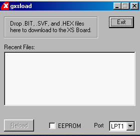
Double click on the GXSLOAD program, which is located in the xstools/bin
directory. This will open the gxsload window (see Figure
3 above). Select the parallel port (e.g. LPT1) and leave the EEPROM
box unchecked.
-
You can now drop the configuration file of the design you want to download
into the window. This is done by going to the directory in which you stored
your design corresponding to the version and revision you would like to
download (e.g. C:\MY_DIR\MY4ADD\XPROJ\Ver\Rev) and selecting the configuration
file, my_proj.svf. Drag and drop the my_proj.svf file into
the "gxsload window". The download process will begin. This may take several
seconds.
6. TESTING
You are now ready to test the design.
-
When using the Digilab board, set the general purpose switches SW1-SW8
in the zero position. The units display should show 0.
-
What do you notice? Are all four seven-segment displays showing the same
results? If so, why is that the case (hint: see the Digilab Board discription)?
How can you prevent the first three displays from showing the units digit?
Go ahead and switch off these three displays. Be careful not to short outputs
together since that will damage the FPGA! If you are not sure check with
the TA.
-
Once the display is working properly (only the 4th display shows the units
digit), change the switch settings for the A and B input signals and check
that the display for the units digit show the correct sum. Also check the
TENS digit (displayed on LD1). Does the ERROR signal goes on when needed?
-
Write the results of the testing down in your lab notebook.
-
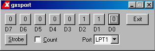
For the XS40 board, test signals are applied through the parallel
cable using the GXSPORT utility (in the XSTOOLS/BIN directory,
click on GXSPORT) shown in Figure 5. In the GXSPORT window, set the
value of the data bits corresponding to the input signals as defined in
the user constraint file (e.g. input A1 is connected to port D0, etc.).
Figure 5: GXSPORT window for applying test signals through the parallel
port. (Screen clip from the XESS (TM) GXSTools).
You will be able to apply the four bits of the A and B input signals.
However, the 7-segment display can only show the digit corresponding to
the units, unless you add an external LED for the tens digit. This can
be easily done by placing the XS40 board on a protoboard and connecting
a LED diode between the pin corresponding to the tens digit (e.g. pin no.
3) and the ground (pin 52). Place a resistor of about 330 ohm in series
with the diode to limit the current. You can do the same for the ERROR
signal.
-
For the FPGA demoboard: Set all the switches SW3 in the zero position
(i.e. left hand side pushed down). You should see 0 displayed on the right
hand side display U8. Next set the switches according to the different
BCD representations of the digits 0 to 9 for the inputs A and B and check
the 7-segment displays. Verify proper operation and write the results down
in your lab notebook. Also check the ERROR signal if implemented.
-
For the XS95 board, test signals are applied through the parallel
cable using the GXSPORT utility (in the XSTOOLS/BIN directory, click on
GXSPORT) shown in Figure 4. In the GXSPORT window, set the value of the
data bits corresponding to the input signals as defined in the user constraint
file (e.g. input A1 is connected to port D0, etc.). You will be able to
apply the four bits of the A and B input signals. However, the 7-segment
display can only show the digit corresponding to the units, unless you
add an external LED for the tens digit or used the decimal point of the
7-segment display. This can be done easily by placing the XS95 board on
a protoboard and connecting a LED diode between the pin corresponding to
the ERROR signal (e.g., pin no. 4 which is a free pin) and the ground (pin
49). Place a resistor of about 560 ohm in series with the diode to limit
the current. You can do the same for the ERROR signal.
After you have convinced yourself that the circuit works properly, five
a demo to the lab instructor and have him sign
off in your lab notebook. The demo is due on the day the lab
is scheduled.
Copy your project back to your persopnal computer account for future
use. If you have created more than one version or revision during the Design
Implementation, you should delete the version that you don't need and keep
only the latest one. These files take up a lot of space. To delete an older
revision, go to the Design Manager window, select the revision you want
to delete and go to the PROJECT->DELETE revision menu (NOTE do not delete
the project!!!). You can also easily zip the project: in the Project Manager
window, go to FILE-> ARCHIVE Project. This will zip the entire project,
including all the project libraries needed for the current project. You
can now save the project in your directory. The archived project is also
handy when you need to email it to somebody else.
Put your name on the Schematic . Take a sreen capture of the top
level schematic to include in your report.
Hand-in (at the start of next lab)
You must hand in a short lab report that contains the following:
The lab report is an important part of the laboratory. Write it carefully,
be clear and well organized. It is the only way to convey that you did
a great job in the lab. It is preferred (but not necessary) that you type
the lab report. This report will count for 75 points and the pre-lab questions
for 25 points.
Go to theVHDL Primer,
ABEL
Primer; go to Common Mistakes
Created by Jan Van der Spiegel;
September 25, 1997; Updated October 1, 2001.
Copyright, Jan Van der Spiegel, 2001.
 th visitor since 10/3/99